Because of the holidays, TI E2E™ design support forum responses will be delayed from Dec. 25 through Jan. 2. Thank you for your patience.

This thread has been locked.

If you have a related question, please click the "Ask a related question" button in the top right corner. The newly created question will be automatically linked to this question.

Re: CC debugger connectivity to CC2545 chip

Other Parts Discussed in Thread: CC2530, CC2545, CC2538

hi sir,
1)when I was connecting the cc debugger to cc2530 module ,the led in cc debugger glows in green color and it was connected.
when it will connected to cc2545 module ,the led glows in red color and the chip was not detected.
no chip was detected message was appearing in smart rf studio.

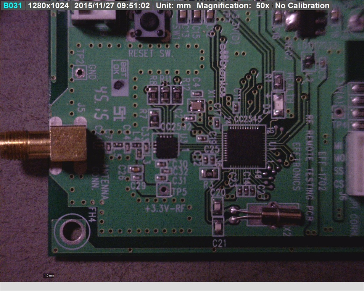
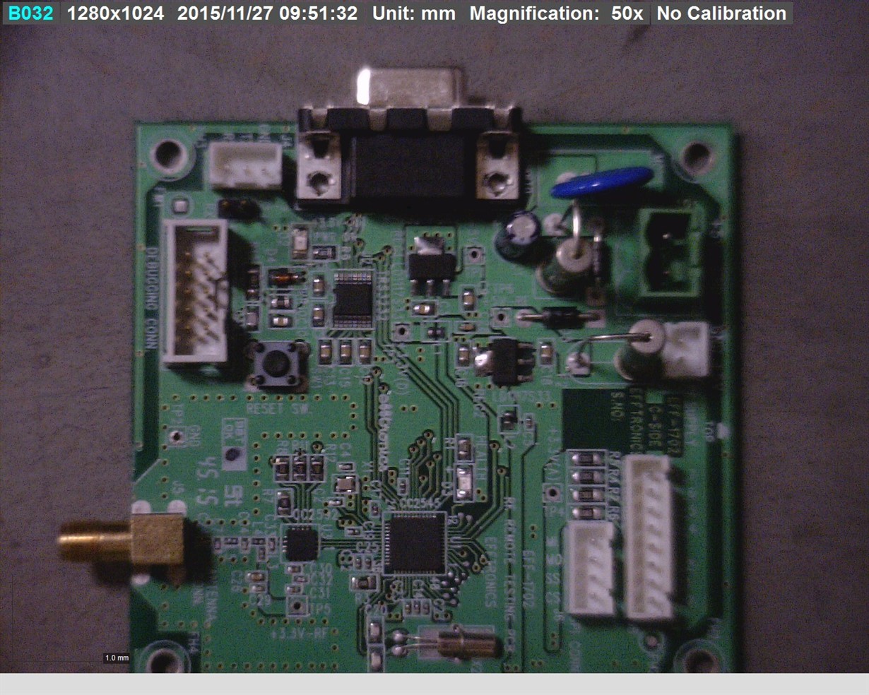
I am attaching my cc2545 hardware design sir. please verify the design sir and please tell where was the problem.

8562.EFF-1702 VER1.0.pdf

I am connecting j9 connector to the Ccdebugger.

Awaiting for your reply,

Regards,

Manikanta.k

  • Hi,

    I observed that you shorted J9-9 and J9-2.

    J9-9 is an internal 3V3 from the CC Debugger, which is used to source the other external devices. It may not have enough power to drive high power consuming external devices.

    In your case, remove the connection from J9-9 on your board, power-up your board from an external supply make sure you have a voltage (3V3) on J9-2. Connect CC Debugger to your board, Press the RESET button on CC Debugger and observe the LED on CC Debugger.

    Thanks,

    PM

  • Hi Sir,

    Thank you for earlier reply,

    I will disconnect it and observe the led I will drop the status .

    Regards,

    Manikanta. K

  • Hi Sir,

    I disconnect the J9-9 on my board and I confirm the voltage on j9-2 pin as 3V3.Then I was connected to the cc debugger .After this connection we pressed the reset

    Still the led was glowing in red color.

    is there any other bug in the circuit sir?

    regards,

    Manikanta.K

  • Hi,

    Please check the Crystal X1 (32MHz), if it is oscillating or not?

    Thanks,

    PM

  • Hi Sir,
    Thank you for your earlier reply.
    Ok sir. I will check and droup the status sir.
    Regards,
    Manikanta.k
  • Hi sir ,

    I was connected  the 32Mhz oscillator to the default pins(26 and 27) of the cc2545 chip. After power on the board I kept the probes to the first pin of crystal and to the ground no wave form was generating sir.

    In the part of troubleshooting I removed the crystal in my board and replace in the other board (cc2538 board) .the wave was generated that mean crystal was in working condition.

    could you please verify the  schematic which was attached in the above post .where was the problem?

    or else is there any steps needed to do before or after power on the board. 

    Regards,

    Manikanta.K

  • Hi,

    How many boards you have? Does all the boards behave the same way?

    Do you have our EM?

    You can measure both DC Resistance and DC voltages on your board and compare with our EM board ( if you have it).

    Did you measure the DC voltage / Resistance on the Crystal pins?

    Yes, I checked your schematic and it looks OK.

    Thanks,

    PM

  • Hi Sir,

    I had 6 boards.In those two are mounted with components.

    Remaining four are bare pcbs.

    In  2 boards the crystal behavior was same sir.No wave was generating.

    No I didn't had the cc2545 em.

    II will check the voltage and resistance on the crystal pins and I will drop the status sir.

    Regards,

    Manikanta. K

  • hi sir,

    I was check the voltage and resistance at pins of crystal as follows:

    For voltage: Connected the probe to the first pin and to the ground (result was (40 -50)mV sir)

    For resistance: Connected the probe to the first and third pin of the crystal(result was 300Kohm)

    Is this procedure was a correct or not sir?

    Could you please check the voltage and resistance at crystal pins for your CC2545em and share the result sir an i will compare the values.

    In the part of troubleshooting ,now I prepared the third board with components and I check the crystal no wave was generating sir. voltage and resistance of this board was same as above.

    Regards,

    Manikanta .k 

  • hi sir,

    I was checked the voltage across VDD,DCOUPL,RESET,RBIAS, are as follows:

    VDD:3.3V

    DCOUPL:1.86V

    RBIAS:1.254V

    RESET:3.3V

    CC2545 section as follows:

    Overall board:

    I am sure that debug signals are connected properly sir.

    After power on I was connected CC debugger as shown in the attached pic.

    We observe the Debug signals and Reset signal in oscilloscope.(All are 3.3V)

    we are not getting clock from crystal after power on the module. By this reason(clock from crystal) CC debugger may be  not detecting the chip.

    How we can load the code or SW  into the chip with out detection of CC debugger?

    IS there any other possible way to load the SW ?.

    Regards,

    Manikanta.K

  • hi sir,

    I was connecting the two cc debuggers at the same time and to the same pc.

    having same usb device id (0000) to the both debugger.

    I am able to open the device control panel on one smart rf studio tool only .

    I am not able to open device control panel on another smart rf studio tool.

    the following window appears :

    Is there any procedure to change the usb device id for the cc debugger.

    or else how to connect the two boards to smart rf studio tool (one as tx and other as RX) at the same time to check the per test?

    Regards,

    Manikanta.K

    K.manikanta

  • Hi,

    You need to measure the resistance from Pin-26 to Ground and Pin-27 to Ground. I think you have CC2538 board. You can compare this resistance with the Resistance on CC2538 board (Pin-34 to Gnd and Pin-35 to Gnd). If you measure a low resistance on these pins that means it is shorting to ground.
    And also measure the DC voltages on Pin-26 and Pin-27 and compare with CC2538 (Pin-34 and Pin-35).

    First the Oscillator should work to generate a clock otherwise the chip doesn't function to load the software.

    Thanks,
    PM
  • Hi sir,

    I  interfaced the cc2592(power extender) to the I/O pins of cc2545 chip as following:


    PA_EN -> P0_1

    LNA_EN--> P0_0

    HGM--->P2_0


    I  connected the 2 boards to the PC with 2 cc debuggers to do the per test in smart rf studio tool.

    The device Id's of cc debuggers as follows are 0000 and 8450

    Initially I kept 0000 as TX and 8450 as RX .In this case communication was achieved

    In vice versa case also communication was achieved.

    My query was there is no option for selecting the range extender in Device control panel in smart rf studio tool.

    But cc2592 was mounted on my 2 boards.

    Could you please explain  how data transfer and reception is working without control of cc2592 chip which is in between CC2545 and Antenna.?


    K.manikanta

  • Hi sir,

    I  interfaced the cc2592(power extender) to the I/O pins of cc2545 chip as following:


    PA_EN -> P0_1

    LNA_EN--> P0_0

    HGM--->P2_0


    I  connected the 2 boards to the PC with 2 cc debuggers to do the per test in smart rf studio tool.

    The device Id's of cc debuggers as follows are 0000 and 8450

    Initially I kept 0000 as TX and 8450 as RX .In this case communication was achieved

    In vice versa case also communication was achieved.

    My query was there is no option for selecting the range extender in Device control panel in smart rf studio tool.

    But cc2592 was mounted on my 2 boards.

    Could you please explain  how data transfer and reception is working without control of cc2592 chip which is in between CC2545 and Antenna.?