Hi,
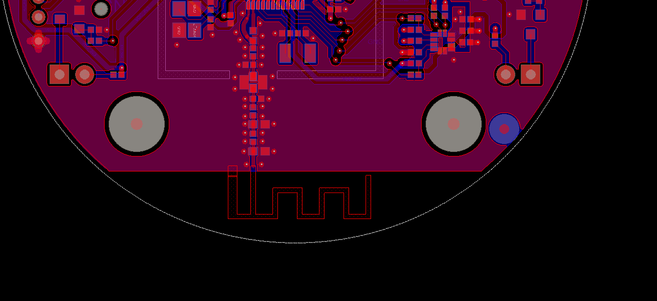
I am referring AN043 for PCB antenna design. we are not getting any response with 2 layer 1.6 mm thickness PCB during Antenna Simulation on CST tool.
We are placing Antenna on top layer and providing sufficient Keep out area(Void),we are providing GND plane on both Top and Bottom layer.
Attaching image for your reference.Please provide your expertise views on this and recommend how can we possibly do it better.