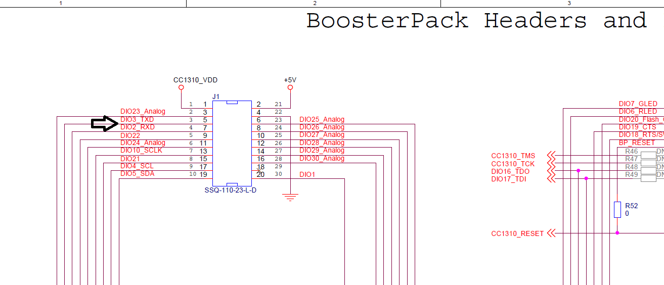
Just noticed when probing around with a multimeter-
J1.3, aka DIO2, is normally the MCU's RXD pin, but it routes to the bottom side of the "TXD>>" jumper in the XDS jumper block.
Likewise J1.4, aka DIO3, routes to the "<<RXD" jumper in the XDS jumper block. That is backwards as per the boosterpack standard and the RTOS defaults:
#define Board_UART_RX IOID_2 /* RXD */
#define Board_UART_TX IOID_3 /* TXD */
I haven't checked the schematic but the backchannel UART does work, so I assume the physical routing is correct, just the silkscreen labels are backwards.