This thread has been locked.

If you have a related question, please click the "Ask a related question" button in the top right corner. The newly created question will be automatically linked to this question.

CC2500: simulation for RF Path

Part Number: CC2500

Hi Everyone..

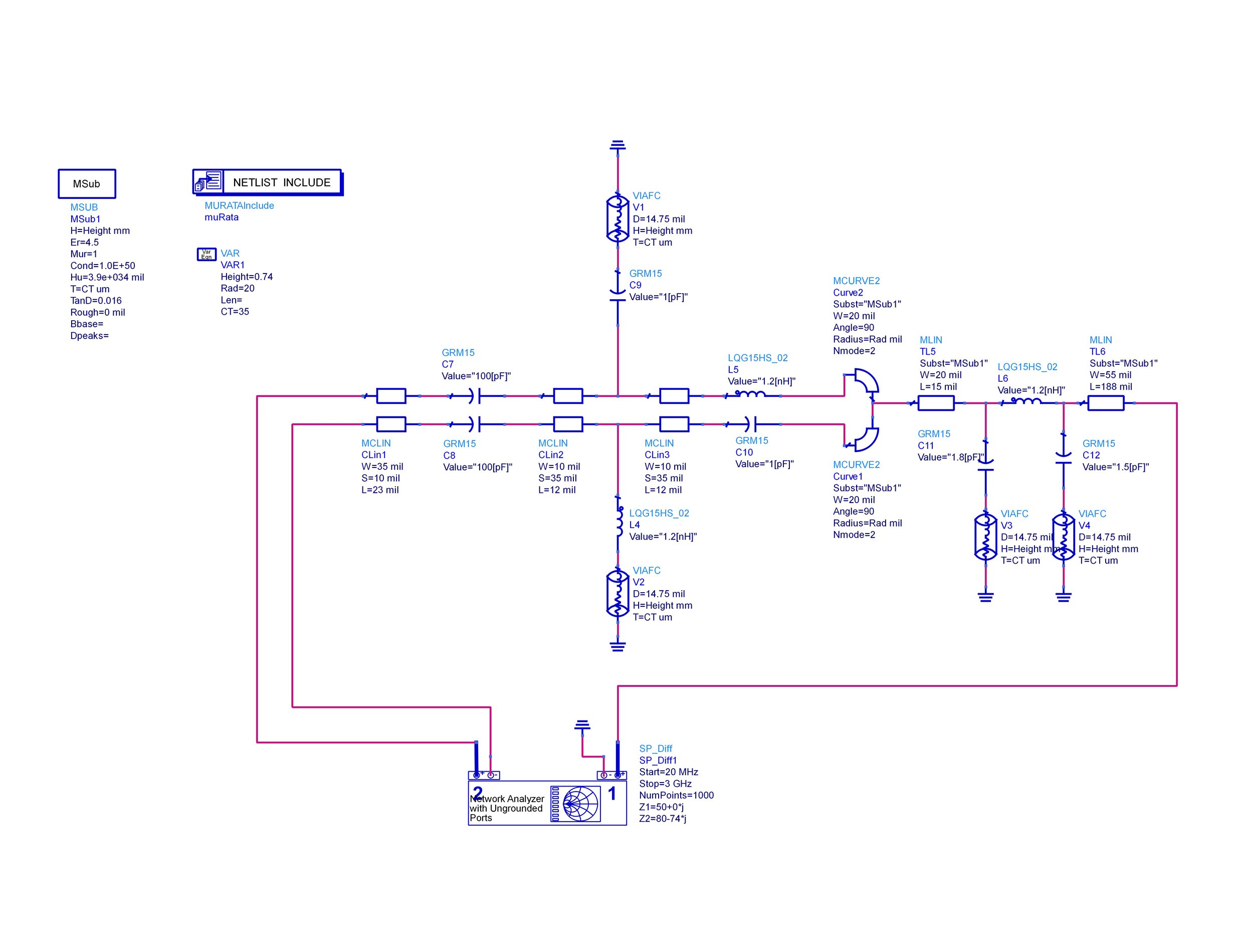
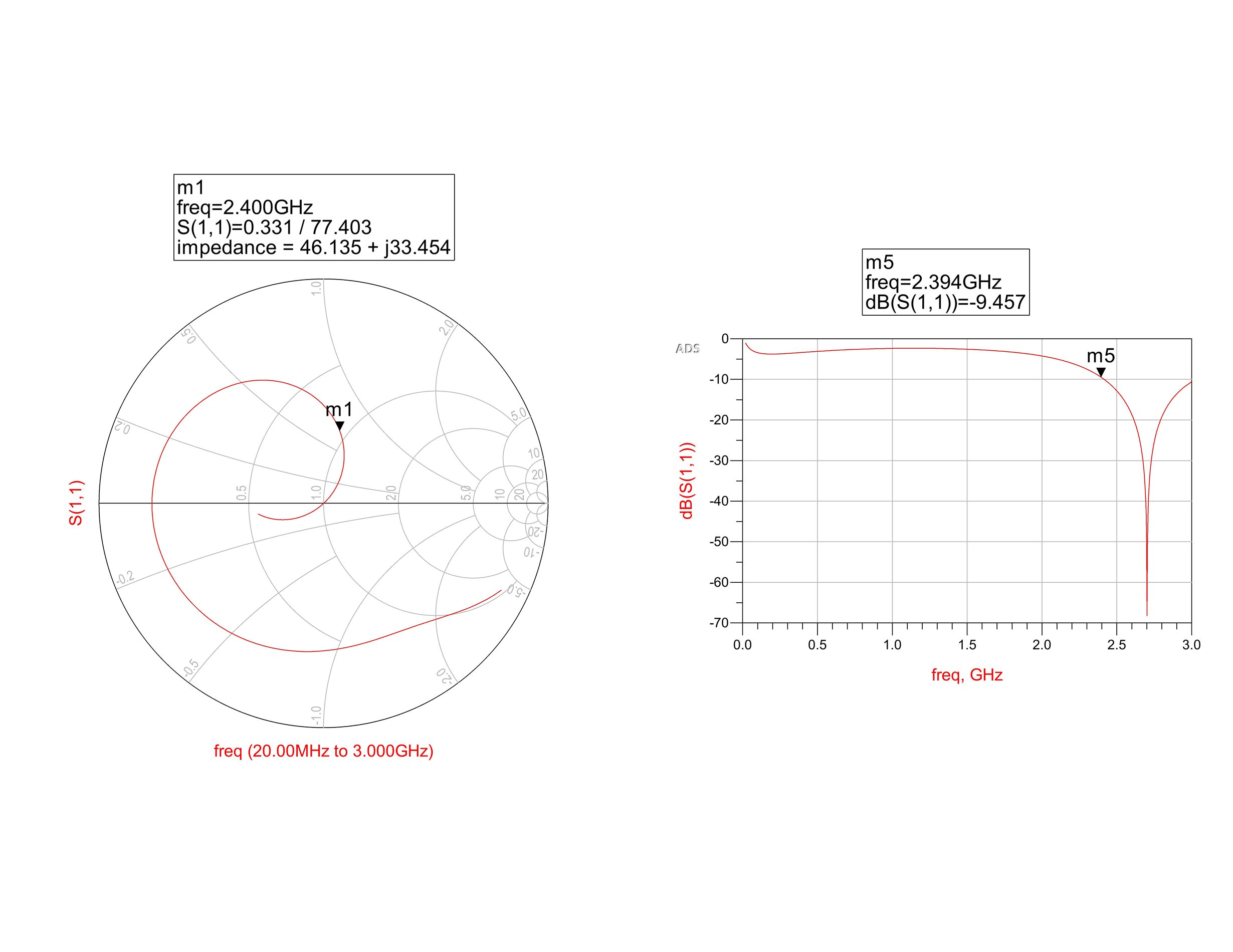
I revere to application note AN068 to make simulation for RF Path of CC2500 ( please find the attached pictures for simulation result)..

From the datasheet 

The passive matching/filtering network connected to CC2500 should have the following differential impedance as seen from the RFport (RF_P and RF_N) towards the antenna:

Zout = 80 + j74 Ω

and I use gerber viewer to capy the width and length of TL (( without pads overlapping )) from reference design.

My Question:

1- why the output impedance is not 50 ohm??

2- what is the effect of length in impedance value?

3- if I want to change H how to calculate the width of TL specially: Differential lines ?? 

  • RFeng,

    Have you validated that the models of the RF components that you are using are correct, there is a new tool on Murata's website that lets you generate models for the components you have selected.

    I also would recommend setting up a comparison measurement between your model and a TI reference board.

    I think what you will find is the level of detail in your model is not yet good enough to fully model all the parasitics of the PCB.

    Regards,
    /TA

  • Thanks Ms. TA12012

    I modified the design  to use a tool that you mentioned (models of the RF components) and got the same results.

    Maybe the problem in the parameter of (curve and TL) in differential to single-ended part..

    Can you confirm if  is it correct or not ??

    Or Where can I get a ADS simulation file that mentioned in AN068 ??

  • Hello,

    To match the impedance exactly, impedance of traces have to be modeled precisely accounting for the ground plane and this can be done using 3D simulation tools. The actual measured values on PCB are usually slightly different from the simulated values because of tolerances on components and PCB fabrication. Hence, after achieving a close matchon simulation, final optimization is ususally done on the PCB.

    Regards,
  • I have looked for this file, it is not possible to find.

    Regards,
    /TA

  • Thanks Ms. TA12012

    can you help me to check if the parameter of my ADS schematic is match with reference design or not ??!!

    Thanks

  • RFeng, 

    I see many differences between the schematic in the AN068 appnote and your simulation. I suggest getting all the MCLIN configurations aligned first.

  • Most of critical parameters for simulation in schematic in the AN068 appnote defined as variable.. and these variable are not shown in the picture !

  • Another point, there are difference in the lengths of the TL between schematic in the AN068 and the Reference Design.