This thread has been locked.

If you have a related question, please click the "Ask a related question" button in the top right corner. The newly created question will be automatically linked to this question.

Question about TX power,patable

Other Parts Discussed in Thread: CC1101, TEST2

Hi,

I want to transmit an electric wave in 10dBm from 426.3MHz in GFSK now.

 I set 0xc0 in PATABLE[0] to 8 bytes of PATABLE.

PATABLE[0] = 0xc0
PATABLE[1] = 0x00
PATABLE[2] = 0x00
PATABLE[3] = 0x00
PATABLE[4] = 0x00
PATABLE[5] = 0x00
PATABLE[6] = 0x00
PATABLE[7] = 0x00

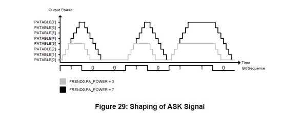
If I want to transmit by 10dBm, Should I set 0x10 in FREND0(0x22) register?

In addition, I write in some TX power data at 8 bytes of PATABLE and will be all right even if I change which PATABLE I use in the PA_POWER[2:0] bit of the FREND0 register?


ex.

PATABLE[0] = 0xc0
PATABLE[1] = 0x50
PATABLE[2] = 0xC7
PATABLE[3] = 0x00
PATABLE[4] = 0x00
PATABLE[5] = 0x00
PATABLE[6] = 0x00
PATABLE[7] = 0x00


  • If FREND[2:0] = 0 you will transmit at the output power defined by PATABLE[0] irrespective of values put into PATABLE[1] to  PATABLE[7].

    In you example, if you write FREND[2:0] = 2 you will ramp up power as follows: 1/8 bit period at 0xC0, 1/8 of a bit period at 0x50, and final value during the transmission at 0xC7 (BTW: this is not a good ramping sequence as the power starts at maximum (0xC0) and ends at a lower value)

  • Hi Sverre,

    Thank you for your reply.

    when I want to take out a wave pattern such as the figure "FREND0.PA_POWER = 7 " in OOK/ASK

    Should I set the TX POWER VALUE in PATABLE[0]~[7]  for good ramping     PA[0] < PA[1] < PA[2] < PA[3] < PA[4] < PA[5] < PA[6] < PA[7] ?

    Thank you for your help.

    kenji

  • The answer to the question is "yes". That is, PA[0] < PA[1] < PA[2] < PA[3] < PA[4] < PA[5] < PA[6] < PA[7].

    The easiest way to get the PATABLE setting is to use SmartRF Studio and tick off "PA ramping". You will then get a PATABLE consisting of 8 entries. 

  • Hi Sverre,

    Thank you for your reply

    I confirmed it by SmartRF04EB for paramping's PATABLE consisting of 8 entries now.

    Thank you so much.

    kenji


  • Is this description valid for FSK/GFSK modulation?

    I have a problem with the 6th harm. -> it is to big, so I am searching for a solution. From the test lab I got the answer that we "switch to strong".

    Could I solve this using PA Table ie set 2 or 3 power grades, to "switch bits gently"


    Thank you.


    PS

    On the picture, is the proposed power limit, ie we shoud stay out of tv band...

    We could solve the problem by setting the lower send power, but we need 10dBm..


  • What is the level of the 6th harmonic and exact frequency ?

    What is your operating frequency and output power level ?

    Regards,   Richard.

  • Thanks for a fast answer.


    We use 868.9 MHz. Harmonic power is visible on the posted picture..


    We use this CC1101 Parameter set:


    const unsigned char A_Link_Config[] = {
        0x06,    //IOCFG2 // relative carrier sense.
        0x2E,    //IOCFG1
        0x02,    //IOCFG0
        0x00,    //FIFOTHR        // ASSERT WHEN TX BUFF 29, AND RX 35
        0x54,    //SYNC1
        0x76,    //SYNC0
        0xFF,     //PKTLEN
        0x84,    //PKTCTRL1
        0x00,    //PKTCTRL0
        0x00,    //ADDR
        0x00,    //CHANNR
        0x08,    //FSCTRL1
        0x00,    //FSCTRL0
        0x21,    //FREQ2
        0x65,    //FREQ1
        0x6A,    //FREQ0
        //0x6A,    //MDMCFG4
        //0x4A,    //MDMCFG3
        //test setting
        0x5C,    //MDMCFG4 // 103149Hz
        0x04,    //MDMCFG3
        0x15,    //MDMCFG2 /// gfsk on
        0x42,    //MDMCFG1 // 8 preamble bytes
        0xF8,    //MDMCFG0
        0x42,    //DEIVATN -> test settings
        //0x47,    //DEIVATN
        0x07,    //MCSM2
        0x30,    //MCSM1        //go to FSTXON mode 0101 0==> go to idle state
        0x18,    //MCSM0        // calibrate every fourth time.
        0x2E,    //FOCCFG
        0x6D,    //BSCFG
        0x04,    //AGCCTRL2
        0x19,    //AGCCTRL1
        0xB2,    //AGCCTRL0
        0x87,    //WOREVT1
        0x6B,    //WOREVT0
        0xFB,    //WORCTRL
        0xB6,    //FREND1
        0x10,    //FREND0
        0xEA,    //FSCAL3
        0x2A,    //FSCAL2
        0x00,    //FSCAL1
        0x1F,    //FSCAL0
        0x41,    //RCCTRL1
        0x00,    //RCCTRL0
        0x59,    //FSTEST
        0x7F,    //PTEST
        0x3F,    //AGCTEST
        0x81,    //TEST2
        0x35,    //TEST1
        0x09    // TEST0
       

    };


    What are the possibilities to reduce the power of the 6 harm, only by changing software( cc1101 parameters)?


    Regards,

    Ervin

  • Hi,

    Is the harmonic spur at 5.2123 GHz or 5.2134 GHz ?

    Regards, Richard.

  • Hi.


    .


    It is 5.2134GHz


    With some hardware changes we pushed 6th under -30dBm (marker 1), and that is (almost) ok, but we are still not satisfied...


    So back to my question, does this PA table ramping system works with FSK/GFSK?


  • The harmonics level is not dependent on whether PA ramping is enabled or not. Please note that when doing compliance testing under En 300 220 you will measure the radiated spurious level. The antenna has a finite BW and will lower the 6th harmonic to well below -30 dBm.


  • Agree also that with a 868 MHz antenna; the radiated level will be significantly lower and PA ramping will not help here.

    With standard multi-layer inductors from Murata the level of the 6th harmonic is usually around -56 dBm conducted with 12dBm output power at 868 MHz so your level seems quite high. If wire wound inductors are used the level can be surpressed furthermore but multi-layer inductors should be sufficient. 

    Check out DN032 (http://www.ti.com/litv/pdf/swra346) concerning the choice of inductors used in the RF structure.

    Regards,   Richard.