This thread has been locked.

If you have a related question, please click the "Ask a related question" button in the top right corner. The newly created question will be automatically linked to this question.

CC8531: Cant communicate with CC8531 using the reference design

Part Number: CC8531
Other Parts Discussed in Thread: CC2590, CC2592

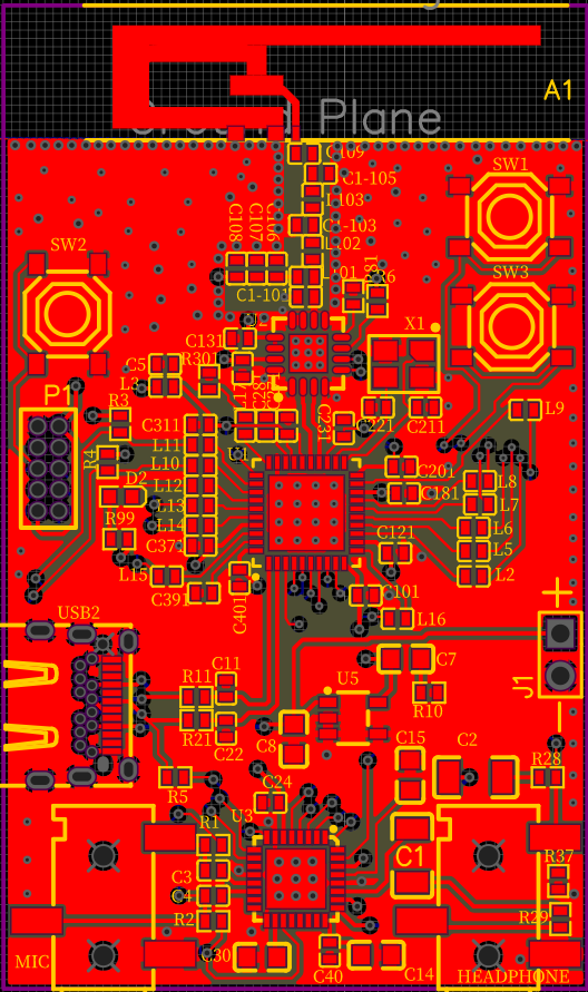
I have implemented the headset reference design for the PurePath CC8531. I made some changes to the power circuit eliminating the charger.

Unfortunately, I cant get it to work. It does not register via USB, nor can I connect to it using the CC Debugger. I understand that I have probably done something wrong, but after checking all the connections I am unable to figure it out. I have gone over all the traces and there are no breaks, also as far as I can tell all the power and ground connections are as they should. I'm really at a loss here

Any help would be greatly appreciated.

See below for the schematic:

  • Hi,

    I would not expect it to show up over USB until you flashed a USB Host image to the device, as such, the first step would be to get the CC Debugger to work.

    I can't find any immediate issue with the schematics, I would make a double and triple check of:

    1) Power, are all power rails (and inputs) there, no shorts on any of these?

    2) Check the 48 MHz crystal, if this do not run, the device will not start up either (not even for the debugger).

  • Hi.

    Thank you for your feedback. I managed to find the fault. I compared the headset reference design to the USB dongle reference design and noticed that pin 9 on the debug port was connected to power of the dongle design, but left unconnected in the headset design. Connecting pin 9 to power solved the problem, and I am able to flash the cc8531 chip. Unfortunately the range of the device turned out to be very disappointing.  I only managed to get something like 30cm of range.

    I am very new to RF and Microwave PCB design so I understand that I have probably made a lot of mistakes in designing the RF part of the device even though I tried to follow whatever I could find in the reference design to the limit of my knowledge. I would greatly appreciate any pointers into what I have done wrong so that I can correct these mistakes. One concrete issue is the TLI inductors on pins 10, 13 and 16 on the CC2590. Also pin 1 is connected in the reference design, but in the datasheet it says its unconnected. 

    I have attached the gerber files to this post.

    Any help would be greatly appreciated.

     Gerber_PCB_2020-07-10_14-45 Master.zip

  • Hi,

    There is a few things to consider but in general, you RF design could do for improvements. I would recommend looking that the layout of the headset (there is a PDF among the design files):

    https://www.ti.com/lit/zip/swrr079

    A few basic things to consider is the impedance of the RF path. You can see that for example the headset has quite some ground clearance around the RF path. how it should look in your case I can not say as it depends on things like the PCB stack-up and specs and you would need to perform your impedance calculations based on this. Personally I use "Saturn PCB toolkit" for my private projects to do my calculations.

    Ideally you would like to simulate your RF matching network as well but assuming you can copy the PCB stack-up used on the headset reference design you should be able to leverage those line widths etc (basically copy the RF design part).

    i would also recommend looking at the RF connection between CC2590 and CC8531, this is a differential signal and you should keep them symmetrical and  matched in length as much as possible (again, the layout in the reference design shows a good example). These should also use correct width+spacing to get the correct differential impedance.

    if doing another run at this, I would also recommend looking into substituting the CC2590 with CC2592. Even while this is not part of the PureParth configuration tool, it would work and it does not depend on the external "trace impedance" like the CC2590 does (it is easier to design with).

    Beside that, take a extra look at return paths etc in the design and make sure to minimize these as much as possible (did not look to close at this). One thing that caught my eye was the ground-plane design around the crystal, you got any special thought around this?

  • Thank you very much for your feedback.

    I will have another go at this taking you feedback into account, including switching to the CC2592. I had that as an idea but was unsure it would work. I'm using PCBWay as my PCB manufacturer and would like to use their standard 4 layer stackup if possible. Both out of convenience but also to understand more about impedance control. Using PCBWays impedance calculator I get very different values than with Saturn PCB toolkit so that will need some further investigation. 

    Regarding the ground plane design under the crystal, I got that from here: https://www.youtube.com/watch?v=14_jh3nLSsU&t=1916s

    Is that design wrong or unnecessary?

    Thank you.

  • Hi,

    Interesting seeing such a difference in calculations. My recommendation is using Saturn to perform the calculations and aim to have a value that is about 5-10% higher then what you expect. This offset is to account for the impact of the solder mask which would further lower your impedance.

    As for the ground plane under the crystal, there is nothing wrong with it but you could consider it a "very cautious" design. It could be helpful if you got a lot of noise in the ground plane but in this particular case, you should be fine without it. That said, you could leave it in if you want to, it should also not hurt your performance. 

  • Hi.

    I have made a new design and tried to include all the recommendations I was given. I'm using PCBWays standard stackup as shown above

    1) I have substituted the CC2590 with a CC2592

    2) Used the PCB Toolkit calculator and calculated the impedance for both the USB (90 Ohm Zdiff / 45 Ohm Z0). The actual values became 88.649 and 45.447 Ohms. W=0.17, S=0.34, H=0.11

    3) Calculated the impedance for the differential pair between CC8531 and CC2592 (100 Ohm Zdeiff / 50 Ohm Z0). Actual values became 99.9 and 54.1 Ohms. W=0.12, S=0.21, H=0.11

    4) Added some space between the RF track and the top ground plane. Tried to make it look like the reference design for CC2592 by eye.

    5) Removed the "Special ground plane" under the crystal

    Regarding the CC2592. I see that in the reference design it includes an EMI shield. Is this a must or can I get by without it? I'm having a hard time making it fit on my design. Would have to redo the whole thing.

    I have included the new Gerbers and would very much appreciate if someone could have a look. Would very much like to get this thing to work :)

    Thank you!Gerber_PCB_2020-07-10_14-45 Master (1).zip 

  • Hi, 

    Sorry for the delay, there is much to do these days. I have made a small review of the layout and I do have a few pointers. To start with, I would recommend looking closer at this HW design document with some considerations: 

    http://www.ti.com/lit/pdf/swra640

    Generally, I would advice you to look over the following things more closely:

    • VDD connections. You seem to sometime filter VDD and sometimes not. Consider your CC2592 setup for example. Here you pull VDD straight from your "VDD Plane" which also means that any leaking harmonics could propagate into this plane which could case unwanted issues with EMI (as the plane could be considered an antenna of sort). 
    • Decoupling in general. Try to follow the Power -> Cap -> Component topology in the design. Today you sometimes but the via between the decoupling cap. and the component which is not ideal.
    • Try to move the PA closer to the CC85xx chip to minimize the RF path here. Also, consider that the differential lines are not Z0 = 50 Ohm, the output of CC85xx is closer to Z0 = 76 Ohm.
    • Make sure to have GND vias close to the component pads. In your RF network for example, some of the caps do not have a via in connection to the pad while some do. 
    • Yry to move the XTAL a bit closer to the CC85xx if possible.
    • You seem to use quite small tracks in general, I would try to make them a bit larger (to the point where you are still able to make up the design).
    • Avoid the thermal relief on the antenna to GND plane connection points. These serve no purpose as you will not be soldering the antenna anyway and could in worst case impact your performance. 

    Now some of these points might me more or less critical but I would advice to spend some time trying to "clean up" the overall layout. As a colleague once said, a small factor of "OCD" is not a bad things when it comes to doing the layout ;) Here is two pictures highlighting some of the points mentioned above:


  • Thank you so much for the feedback. It's really helpful. I read through the paper you referenced and made some adjustments. I also looked checked all you comments and made changes. The design is clearly still not perfect, but I hope I'm now at a stage where the design will give me a better range than 20 cm :)

    I manged to pull the crystal closer and also pulled the PA closer to the CC8531. I increased the trace width from 01mm to 1.5 mm.

    I also opted to use the same stackup as in the headset reference design, and therefore I also recalculated the impedance of the USB, and RF. A question though, in the headset reference design the RF traces between the cc8531 and the PA is 0.25mm. With that stackup that gives roughly 50Ohm. You pointed out that the impedance should be closer to 76Ohm Z0. If I want to target 76 Z0 and then 152Ohm Zdiff? then I would end up with a trace of w=0.1, s=0.5 with a h=0.175.

    Right now I have them at w=0.25 and s=0.3. Will this work?

    Thanks again for the help so far. It's a steep learning curve for me, but that is part of the fun with this.

    The design is clearly not perfect but I hope I'm getting closer to something that will work, so my question then is, will it work? :)

    I attached a picture of the design and also the updated gerbers.

    Kind regards

    Gerber_PCB_2020-07-10_14-45 Master exp.zip

  • Hi,

    It looks better, here is a few notes to consider (applies generally as well):

    I would adjust the GND plane a bit here. If using thermal expansions like the right most box, try to get connections on three sides. Around C1-101, why did you open up the plane so much here, seems like it is all GND anyway?

    As for the antenna connection, I would suggest you look into removing the thermal relief setting for these GND connections instead of making think traces. Generally, you want to avoid changing the width like that at it could impact RF performance. 

    In the yellow area, I want you to consider the VDD routing. For example, try to switch place on the filter bead and cap. Also, it seems that you have vias down to fan it out to the other side. This is fine but consider using thicker traces and also, looking at the "U1" designator, why do you feel you need to go down to bottom in order to get the power to this pin, it is right there above it already? :)

    The three VDD pins right next to the RF path could also need some additional love, consider using polygons/other arrangement to get a more solid power routing going. 

    The green box is meant to highlight that you could maybe try to get some GND on both sides (I know it is hard) as well as a via or two (and some keep out for the traces).

    Green box -> power to component vs capacitor order. Yellow box: Seems that you are complicating the routing here, seems to me you could align this up, move L9 down and just arrange the vias in another way. I would also avoid routing "under" the inductors if not needed.

    As for the differential lines, you still want Zdiff to be 100 Ohm even if targeting another Z0. As I was not involved in the headset design, I could not really comment on the decisions taken here on the specific line width. From now and then there could be deviations from "text book" examples and there could be reasons for this based on the rest of the layout (for example, GND lanes very close to RF traces could impact impedance further).

    You should see the headset design having the ability to mount an additional match on the diff lines but it was likely found out to not be needed in the final EVM kit. If you try to keep good GND around the RF path, have an "OK" trace -> plane clearance (say 2 times trace width) to minimize impact these have on trace impedance, then you should be OK. You might not be perfect but I would not expect horrible either. 

    Now if you are able to copy the exact PCB stack-up used int he design, then you should be able to leverage the work from this design in terms of traces widths etc.