Other Parts Discussed in Thread: MSP430G2553, , MSP430F5529
Tool/software: Code Composer Studio
Hello,
I want to using the RF430FRL152H & TRF7970ABP+MSP430G2553 to measure the analog signal. I want to implement the following functions:
(1)The ADC in RF430FRL152H samples the analog signal at a sampling frequency of 20Hz~25Hz;
(2)TRF7970ABP+MSP430G2553 obtains signal through RF field and sends it to PC through serial port for real-time and continuous acquisition.
So, there is the code I programmed in RF430FRL152H
-------------------------------------------------------CODE SPACE----------------------------------------------------------------------------
#include <rf430frl152h.h>
#include <string.h>
#include "types.h"

//*****************************FUNCTION PROTOTYPES********************************/
void DeviceInit(void);
void initISO15693(u16_t parameters );
void SetupSD14(unsigned char channel);
//********************************************************************************/
u16_t SamplesBuffer[4];
//u08_t State;

//enum state_type
//{
//    IDLE_STATE              						= 1,
//    ONE_SHOT_TEMP_REFERENCE_SAMPLE_STATE            = 2,
//    ONE_SHOT_TEMP_THERMISTOR_SAMPLE_STATE           = 3,
//};

enum Channel_Types
{
    ADC0_CHANNEL                        = 0x0,
    INTERNAL_TEMPERATURE_CHANNEL        = 0x1,
    THERMISTOR_ADC2_CHANNEL             = 0x2,
    REFERENCE_ADC1_CHANNEL              = 0x3,
};

//*****************************DEFINES *******************************************/
#define CLEAR_BLOCK_LOCKS                            	BIT3
#define FRAM_LOCK_BLOCK_AREA_SIZE  						38
#define FRAM_LOCK_BLOCKS								0xF840  //Address of ISO15693 lock blocks


#define ROM_EUSCI_SUPPORT_ENABLED       BIT2
#define EROM_EUSCI_SUPPORT_DISABLED     0
#define ROM_SENSOR_SUPPORT_ENABLED      BIT7
#define ROM_SENSOR_SUPPORT_DISABLED     0
#define	NFC_BRIDGE_DISABLED 			BIT6
#define	NFC_BRIDGE_ENABLED  			0
#define	EIGHT_BYTE_BLOCK    			BIT0
#define	FOUR_BYTE_BLOCK     			0
#define	FIRST_ISO_PAGE      			BIT1
#define	SECOND_ISO_PAGE     			0

/* Firmware System Control Byte
 *
 *     Bit 0: 	ISOBlockSize				0 - 4 byte,		1 - 8 byte
 *     Bit 1:	Page						0 - page 1, 	1 - page 0 (Effective only for 4-byte block mode)
 *     Bit 2: 	ROMEUSCISupportEnabled		0 - disabled, 	1 - enabled (Forced to 0 on RF430FRL153H)
 *     Bit 3-5: ReservedISO
 *     Bit 6: 	NFCBridgeDisable  			0 - enabled, 	1 - disabled (see note below)
 *     Bit 7:   ROMSensorSupportEnable		0 - disabled, 	1 - enabled (Forced to 0 on RF430FRL154H)
 *
 *     NFC bridge is recommended to be disabled in this project.  Unexpected behaviour can occur,
 *     trying to use it, due to the configuration being setup here.
 *
 *     If eUSCI host controller portion is needed along with the RF functionality, the default project
 *     must be used.  That is NFC cannot be supported in that application (because the I2C/SPI host controller
 *     control registers are in the same place that the NFC file needs to be).  However the rest of the FRAM
 *     memory can be used for storing and reading using ISO15693.
 */
#define FIRMWARE_CONTROL_ADDRESS 	0xF867
#pragma RETAIN(Firmware_System_Control_Byte);
#pragma location = FIRMWARE_CONTROL_ADDRESS
const u08_t Firmware_System_Control_Byte = ROM_SENSOR_SUPPORT_DISABLED + EROM_EUSCI_SUPPORT_DISABLED + NFC_BRIDGE_DISABLED + FOUR_BYTE_BLOCK + FIRST_ISO_PAGE; //0x7F,		// this value sets the firmware system control register

// ROM variables - DO NOT CHANGE !!!
// Declared to protect from use by compiler
/********************************************/
#pragma RETAIN(DS)
#pragma location = 0x1C00
u08_t DS;
#pragma RETAIN(RF)
#pragma location = 0x1C6A
const u08_t RF;
#pragma RETAIN(NRX)
#pragma location = 0x1CA4 //rx
const u08_t NRX[34];
#pragma RETAIN(NTX)
#pragma location = 0x1CC6 //tx
const u08_t NTX[33];
#pragma RETAIN(EL)
#pragma location = 0x1CF2
const u08_t EL;
#pragma RETAIN(PF)
#pragma location = 0x1C0A
const u16_t PF[48];
/********************************************/

#define NDEF_START_ADDRESS	0xF868
#pragma RETAIN(NFC_NDEF_Message);
#pragma location = NDEF_START_ADDRESS;																	// the location of the address
const u08_t NFC_NDEF_Message[21] = {
		// Most of the Android applications will not recognize this message as NDEF at this point, due to the
		// tag not being registered with Android NFC stack.  However ISO15693 RFID communication is supported.
		// Block 0
		0xE1, 		// NDEF Magic Number
		0x40, 		// Version Number, read/write access conditions
		0xF2,//F3*4/8 = 0x79  //0x7E,		// 1008 bytes / 8 = 126 blocks
		0x00,//extended memory //0x00,		// does not support read multiple blocks (limited to only 3 blocks)

		// Block 1
		0x03,		// NDEF Message present
		0x0B,		// Length , 11 bytes
		0xD1,		// Record header
		0x01,		// type length

		// Block 2
		0x07,		// Payload length
		0x55,		// Record Type U (URI)
		0x01, 		// URI header identifier
		0x74,		// 't'

		// Block 3
		0x69,		// 'i'
		0x2E,		// '.'
		0x63,		// 'c'
		0x6F,		// 'o'

		// Block 4
		0x6D,		// 'm'
		0xFE,		// TLV terminator
		0x00,		// Empty don't care
		0x00,		// Empty don't care
};

/*********************** SUMMARY **************************************************************************************************
 * This project only utilizes the RF stack (ISO15693) on the ROM of the RF430FRL15xH. This setup allows the user to make a
 * custom application that is run from FRAM.  Only the RF13M vector that runs the RF stack needs to be pointing to its
 * ROM location.
 */

/**************************************************************************************************************************************************
*   Main
***************************************************************************************************************************************************
*
* Brief :
*
* Param[in] :   None
*
*
* Param[out]:   None
*
* Return :
*
**************************************************************************************************************************************************/

void main()
{
	WDTCTL = WDTPW + WDTHOLD;                   // Stop watchdog

    // ROM RF13M module setup ** The following three lines are needed for proper RF stack operation
    DS = 1; 									// ROM variable needs to be initialized here
    asm ( " CALL #0x5CDA "); 					// Call ROM function ( Initialize function pointers)
    asm ( " CALL #0x5CAC "); 					// Call ROM function ( Check part configuration)


	initISO15693(CLEAR_BLOCK_LOCKS);
	DeviceInit();

	while(1)
	{
		//State = ONE_SHOT_TEMP_REFERENCE_SAMPLE_STATE;
		SetupSD14(ADC0_CHANNEL);
	}
	    //__bis_SR_register(LPM3_bits + GIE); // sampling here two channels, SD14_ADC will wake up twice and store the conversions
											// into samplesBuffer, last conversion will cause this LPM mode to be exited and continue to below.
		//processing can be done on the stored conversions here
		//  SamplesBuffer[0]  = ADC0 conversion result
		__bis_SR_register(LPM3_bits + GIE);
		__no_operation();
}

/*  SetupSD14                                                                    						*
 *  The channel to be sampled (thermistor or reference resistor)                  						*
 *  Function:  This function is setup for sampling either a thermistor or a reference resistor         	*/
void SetupSD14(unsigned char channel)
{
	// setting: channel to be sampled, the programmable amplifier gain (2x), CIC filter, SD14INTDLY0 needed since CIC filter needs atleast two consecutive samples before producing an accurate result
	// SDRATE at fastest result possible but also not the most accurate, also enabled is the SD14RBEN which is the current source into the thermistor and references resistor
    SD14CTL1 = SD14GAIN_0 + SD14FILT__CIC + SD14RATE__CIC32 + SD14INTDLY_0 + channel;

    // clock from ACLK (64kHz from VLO clock), SD14DIV1 is set for divide by 32 times (SD14 needs a 2kHz clock),
    SD14CTL0 = SD14IE + SD14DIV1;     // 2 kHz sampling rate, ACLK source, SVSS ground (.125V), interrupt enable

    SD14CTL0 |= SD14EN;               // SD14 module enabled,
    SD14CTL0 |= SD14SC;               // start the conversion
}

//Set and Read ADC0

#pragma vector=SD_ADC_VECTOR
interrupt void SD14_ADC (void)
{
	switch(__even_in_range(SD14IV,4)) //SD14IV register status:00h-no interrupt pending; 02h-SD14MEM overflow(SD14OVIFG);04h-SD14MEM new result(SD14IFG)
	{
		case SD14IV__NONE: // no interrupt pending
			break;
		case SD14IV__OV: //SD14MEM overflow - SD14OVIFG
			SD14CTL0 &= ~SD14OVIFG; // clear the overflow bit
			break;
		case SD14IV__RES:
			SD14CTL0 &= ~SD14IFG;   // clear the data available interrupt
			SamplesBuffer[0] = SD14MEM0;
			SD14CTL0 |= SD14EN + SD14SC;
             /*if (State == ONE_SHOT_TEMP_REFERENCE_SAMPLE_STATE)
			{
				State = ONE_SHOT_TEMP_THERMISTOR_SAMPLE_STATE;
				SamplesBuffer[0] = SD14MEM0;            // compensation for thermistor current bias error
				SetupSD14(THERMISTOR_ADC2_CHANNEL);              //setup ADC and start the conversion
			}
			else if (State == ONE_SHOT_TEMP_THERMISTOR_SAMPLE_STATE)
			{
				SamplesBuffer[1] = SD14MEM0;            // compensation for thermistor current bias error
				SD14CTL0 &= ~SD14EN; //disable the SD14 until it is restarted if using consecutive readings by the timer
				State = IDLE_STATE;
				//conversion completed, data available
				__bic_SR_register_on_exit(LPM4_bits);  	//exit LPM mode after this interrupt
			}*/
			break;
	}
}
/**************************************************************************************************************************************************
*  DeviceInit
***************************************************************************************************************************************************
*
* Brief : Initialize the clock system and other settings
*         Patchable function
*
* Param[in] :   parameters:  has these independent options
*                            INITIALIZE_DEVICE_CLOCK_SYSTEM - initializes the clock system
*                            POPULATE_INTERRUPT_VECTOR_IN_INITIALIZATION - populate the default interrupt vectors and recalculate their CRC
*
* Param[out]:  None
*
* Return  None
*
* Patchable :   Yes
**************************************************************************************************************************************************/
void DeviceInit(void)
{
	P1SEL0 = 0xF0; //keep JTAG
	P1SEL1 = 0xF0; //keep JTAG
    P1DIR &= ~0xEF;
    P1REN = 0;

    CCSCTL0 = CCSKEY;                        // Unlock CCS

    CCSCTL1 = 0;                             // do not half the clock speed
    CCSCTL4 = SELA_1 + SELM_0 + SELS_0;      // Select VLO for ACLK and select HFCLK/DCO for MCLK, and SMCLK
    CCSCTL5 = DIVA_2 + DIVM_1 + DIVS_1;      // Set the Dividers for ACLK (4), MCLK, and SMCLK to 1
    CCSCTL6 = XTOFF;                         // Turns of the crystal if it is not being used
    CCSCTL8 = ACLKREQEN + MCLKREQEN + SMCLKREQEN; //disable clocks if they are not being used

    CCSCTL0_H |= 0xFF;                       // Lock CCS

  return;
}

/**************************************************************************************************************************************************
*  initISO15693
***************************************************************************************************************************************************
*
* Brief : Initializes the RF Stack
*
* Param[in] :   parameter - the configuration to setup the ISO15693 (option to clear the lock blocks)
*
* Param[out]:   None
*
* Return        None
**************************************************************************************************************************************************/
void initISO15693(u16_t parameters )
{

  // enable interrupts  ** Do not change the following two lines, needed for proper RF stack operatoin
  RF13MCTL |= RF13MTXEN + RF13MRXEN + RF13MRFTOEN; 	// set up rx and tx functionality on RF13M module
  RF13MINT |= RF13MRXIE + RX13MRFTOIE;  			// enable interrupts on RX and on timeout and over and under flow checking

  if (parameters & CLEAR_BLOCK_LOCKS )
  {
    //initializeBlockLocks();   //inline function
    memset ((u08_t *) FRAM_LOCK_BLOCKS, 0xFF, FRAM_LOCK_BLOCK_AREA_SIZE);     //block is locked with a zero bit, clears FRAM and RAM lock blocks
  }
}

//#pragma vector = RFPMM_VECTOR
//__interrupt void RFPMM_ISR(void)
//{
//}
//
//#pragma vector = PORT1_VECTOR
//__interrupt void PORT1_ISR(void)
//{
//}
//
//#pragma vector = SD_ADC_VECTOR
//__interrupt void SD_ADC_ISR(void)
//{
//}
//
//#pragma vector = USCI_B0_VECTOR
//__interrupt void USCI_B0_ISR(void)
//{
//}
//#pragma CODE_SECTION(RF13M_ISR, ".fram_driver_code")  // comment this line for using ROM's RF13M ISR, uncomment next one, see .cmd file for details
#pragma CODE_SECTION(RF13M_ISR, ".rf13m_rom_isr") 		// comment this line for creating a custom RF13M ISR that will exist in FRAM, bypassing ROM's, uncomment previous
#pragma vector = RF13M_VECTOR
__interrupt void RF13M_ISR(void)
{
	// Right now this vector is pointing to the ROMs firmware location that runs the RF stack.
    // Entering code here will, without changing the CODE_SECTION lines
	// above, will cause an error.
    // Changing the code section above will cause the ROM RF stack to be bypassed.  New handler will need to be created.
}

//#pragma vector = WDT_VECTOR
//__interrupt void WDT_ISR(void)
//{
//}
//
//#pragma vector = TIMER0_A1_VECTOR
//__interrupt void TimerA1_ISR(void)
//{
//}
//
//#pragma vector = TIMER0_A0_VECTOR
//__interrupt void TimerA0_ISR(void)
//{
//}
//
//#pragma vector = UNMI_VECTOR
//__interrupt void UNMI_ISR(void)
//{
//}
//
//#pragma vector = SYSNMI_VECTOR
//__interrupt void SysNMI_ISR(void)
//{
//}
---------------------------------------------------CODE SPACE----------------------------------------------------------------
I have those question
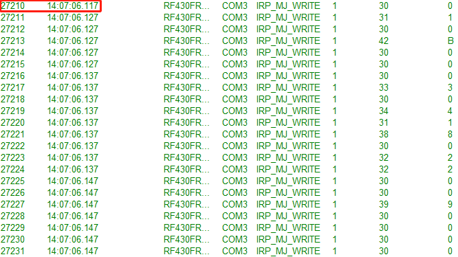
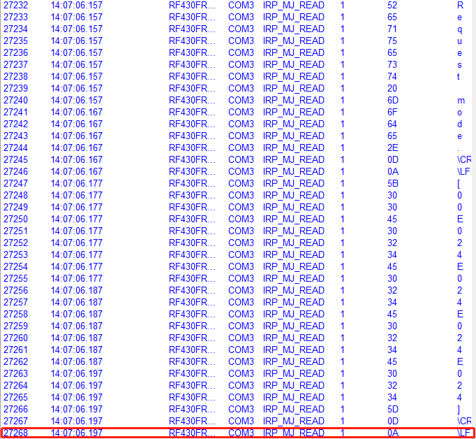
(1)Is my code correct, why can't I achieve continuous and uninterrupted data collection?
(2)Is my ADC set correctly? Can I use some serial assistants to get the data?


