This thread has been locked.
If you have a related question, please click the "Ask a related question" button in the top right corner. The newly created question will be automatically linked to this question.
Hi,
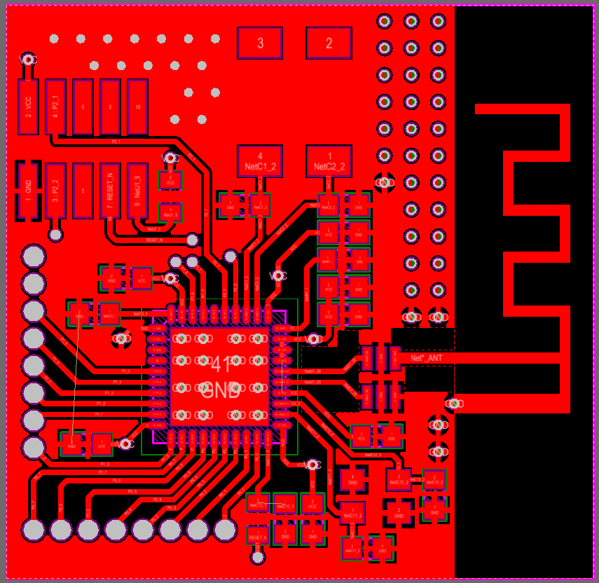
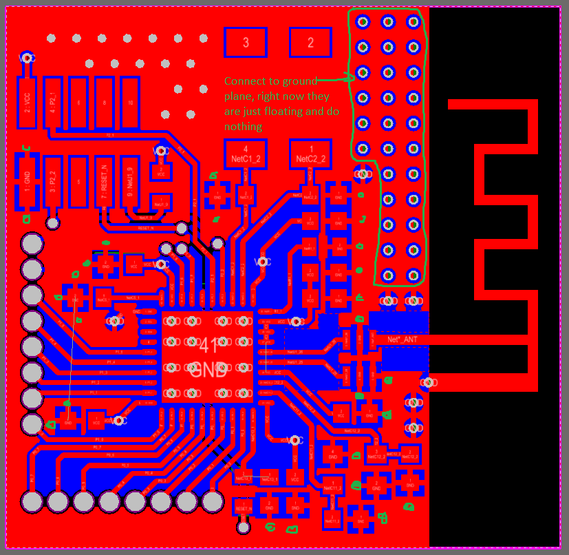
I am using CC2541 + Balun 2450BM15A0002 + MIFA antenna. I'm following antenna dimensions mentioned in swra117d. I'm also following recommended balun design from manudacturer. I'm considering following design things mentioned by TI and other manufacturers in general.
- Solid ground plane underneath CC2541 antenna pins and balun.
- No solid copper region underneath pcb antenna on any layer. I'm using 4 layer design as mentioned in CC2541 Keyfob's Read me file. should there be GND plane below pcb antenna?
- placed lots of vias spaced apart 1.25mm near antenna section.
- Top and Bottom layer are filled with copper pour. Both connected using lots of vias.
- Both crystal and decoupling capacitors are placed as closely as possible.
Questions:
- PCB Antenna's feed line is connected to Balun's antenna pin and pcb antenna's other part is connected to GND. How do I mention this in Altium. Its giving me error. I used solid fill region to make pcb antenna, is it right tool to use?
- Via near antenna section, should these be drilled to GND plane underneath the RF section or should these via be connected to Copper pour on Bottom layer?
Spandan89,
Answers inline:
Solid ground plane underneath CC2541 antenna pins and balun.
- No solid copper region underneath pcb antenna on any layer. I'm using 4 layer design as mentioned in CC2541 Keyfob's Read me file. should there be GND plane below pcb antenna?
- placed lots of vias spaced apart 1.25mm near antenna section.
- Top and Bottom layer are filled with copper pour. Both connected using lots of vias.
- Both crystal and decoupling capacitors are placed as closely as possible.
Questions:
- PCB Antenna's feed line is connected to Balun's antenna pin and pcb antenna's other part is connected to GND. How do I mention this in Altium. Its giving me error. I used solid fill region to make pcb antenna, is it right tool to use?
- Via near antenna section, should these be drilled to GND plane underneath the RF section or should these via be connected to Copper pour on Bottom layer?
Regards,
/TA
Hi,
Really appreciate your quick reply.
Here is updated pcb layout.
I have defined polygon pour cutout area on TOP, GND plane, POWER Plane. I havent defined cutout area on BOTTOM layer. You can see blue area underneath CC2541 pins and balun. is that okay? should I define cutout region there too?
I have defined those via (near ANTENNA section) from TOP to GND plane.
I have added via stitching (top left corner). these via connect TOP and BOTTOM copper pour.
TOP and BOTTOM Layout
TOP Layout
BOTTOM Layout
GND Plane
POWER Plane
One more thing, I havent added pi netowork for antenna tuning. I have made sure that there is a 50 ohm tace from balun to antenna's feed point. is it good practice to add antenna tuning network? Any other suggestions are welcome.
Thanks again.