


Other Parts Discussed in Thread: WMBUS
Hi,
We have a WM-Bus receiver in mode Normal design with the CC1125 radio and work fine.
Know the recveiver must be always on in recepcion mode, but the consumption is very high (26mA).
We are trying to configurate the module in sniff mode, to reduce the current consumption.
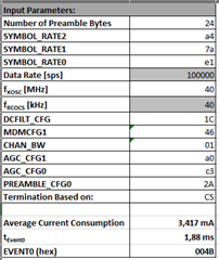
We follow the AN swra428a and configurate the module registers with the smartRF studio7.
WHen the module is in Normal mode, we received all frame from the meters.
When we configurate the module in sniff Mode don´t receive frames, only a 1-2%.
We calculatethe timers Tevent0 throught the excel CC112x_RX-Sniff_Mode.xlxs, always with the same result:
The meters send a frame ever 11 sec.
We try with the termination CS o PQT.
In Normal Mode we use this registers:
// Rf settings for CC1125
RF_SETTINGS code rfSettings = {
0xB0, // IOCFG3 GPIO3 IO Pin Configuration
0x06, // IOCFG2 GPIO2 IO Pin Configuration
0xB0, // IOCFG1 GPIO1 IO Pin Configuration
0x40, // IOCFG0 GPIO0 IO Pin Configuration
0x00, // SYNC3 Sync Word Configuration [31:24]
0x00, // SYNC2 Sync Word Configuration [23:16]
0x54, // SYNC1 Sync Word Configuration [15:8]
0x3D, // SYNC0 Sync Word Configuration [7:0]
0x0B, // SYNC_CFG1 Sync Word Detection Configuration Reg. 1
0x0B, // SYNC_CFG0 Sync Word Length Configuration Reg. 0
0x48, // DEVIATION_M Frequency Deviation Configuration
0x06, // MODCFG_DEV_E Modulation Format and Frequency Deviation Configur..
0x1C, // DCFILT_CFG Digital DC Removal Configuration
0x19, // PREAMBLE_CFG1 Preamble Length Configuration Reg. 1
0x33, // FREQ_IF_CFG RX Mixer Frequency Configuration
0x46, // IQIC Digital Image Channel Compensation Configuration
0x01, // CHAN_BW Channel Filter Configuration
0x05, // MDMCFG0 General Modem Parameter Configuration Reg. 0
0xA4, // SYMBOL_RATE2 Symbol Rate Configuration Exponent and Mantissa [1..
0x7A, // SYMBOL_RATE1 Symbol Rate Configuration Mantissa [15:8]
0xE1, // SYMBOL_RATE0 Symbol Rate Configuration Mantissa [7:0]
0x20, // AGC_REF AGC Reference Level Configuration
0x19, // AGC_CS_THR Carrier Sense Threshold Configuration
0xA9, // AGC_CFG1 Automatic Gain Control Configuration Reg. 1
0xCF, // AGC_CFG0 Automatic Gain Control Configuration Reg. 0
0x00, // FIFO_CFG FIFO Configuration
0x12, // FS_CFG Frequency Synthesizer Configuration
0x7A, // PA_CFG0 Power Amplifier Configuration Reg. 0
0x4E, // PKT_LEN Packet Length Configuration
0x00, // IF_MIX_CFG IF Mix Configuration
0x22, // FREQOFF_CFG Frequency Offset Correction Configuration
0x56, // FREQ2 Frequency Configuration [23:16]
0xE5, // FREQ1 Frequency Configuration [15:8]
0x1E, // FREQ0 Frequency Configuration [7:0]
0x05, // IF_ADC0 Analog to Digital Converter Configuration Reg. 0
0x00, // FS_DIG1 Frequency Synthesizer Digital Reg. 1
0x5F, // FS_DIG0 Frequency Synthesizer Digital Reg. 0
0x00, // FS_CAL2 Frequency Synthesizer Calibration Reg. 2
0x40, // FS_CAL1 Frequency Synthesizer Calibration Reg. 1
0x0E, // FS_CAL0 Frequency Synthesizer Calibration Reg. 0
0x2A, // FS_CHP Frequency Synthesizer Charge Pump Configuration
0x03, // FS_DIVTWO Frequency Synthesizer Divide by 2
0x33, // FS_DSM0 FS Digital Synthesizer Module Configuration Reg. 0
0x17, // FS_DVC0 Frequency Synthesizer Divider Chain Configuration ..
0x50, // FS_PFD Frequency Synthesizer Phase Frequency Detector Con..
0x6E, // FS_PRE Frequency Synthesizer Prescaler Configuration
0x14, // FS_REG_DIV_CML Frequency Synthesizer Divider Regulator Configurat..
0xAC, // FS_SPARE Frequency Synthesizer Spare
0x0E, // XOSC5 Crystal Oscillator Configuration Reg. 5
0xC7, // XOSC3 Crystal Oscillator Configuration Reg. 3
0x07, // XOSC1 Crystal Oscillator Configuration Reg. 1
0x58, // PARTNUMBER Part Number
0x23, // PARTVERSION Part Revision
0x10, // MODEM_STATUS1 Modem Status Reg. 1
0x00, // XOSC_TEST1 Crystal Oscillator Test Reg. 1
0X08, // WOR_CFG1
0x21, // WOR_CFG0
0x00, // WOR_EVENT0_MSB
0x00, // WOR_EVENT0_LSB
//
In SNIFF Mode:
// Rf settings for CC1125
RF_SETTINGS code rfSettings = {
0xB0, // IOCFG3 GPIO3 IO Pin Configuration
0x13, // IOCFG2 GPIO2 IO Pin Configuration
0xB0, // IOCFG1 GPIO1 IO Pin Configuration
0x40, // IOCFG0 GPIO0 IO Pin Configuration
0x00, // SYNC3 Sync Word Configuration [31:24]
0x00, // SYNC2 Sync Word Configuration [23:16]
0x54, // SYNC1 Sync Word Configuration [15:8]
0x3D, // SYNC0 Sync Word Configuration [7:0]
0x0B, // SYNC_CFG1 Sync Word Detection Configuration Reg. 1
0x0B, // SYNC_CFG0 Sync Word Length Configuration Reg. 0
0x48, // DEVIATION_M Frequency Deviation Configuration
0x06, // MODCFG_DEV_E Modulation Format and Frequency Deviation Configur..
0x1C, // DCFILT_CFG Digital DC Removal Configuration
0x31, // PREAMBLE_CFG1 Preamble Length Configuration Reg. 1
0x2A, // PREAMBLE_CFG0 Preamble Detection Configuration Reg. 0
0x33, // FREQ_IF_CFG RX Mixer Frequency Configuration
0x46, // IQIC Digital Image Channel Compensation Configuration
0x01, // CHAN_BW Channel Filter Configuration
0x46, // MDMCFG1 General Modem Parameter Configuration Reg. 1
0x05, // MDMCFG0 General Modem Parameter Configuration Reg. 0
0xA4, // SYMBOL_RATE2 Symbol Rate Configuration Exponent and Mantissa [1..
0x7A, // SYMBOL_RATE1 Symbol Rate Configuration Mantissa [15:8]
0xE1, // SYMBOL_RATE0 Symbol Rate Configuration Mantissa [7:0]
0x20, // AGC_REF AGC Reference Level Configuration
0xF6, // AGC_CS_THR Carrier Sense Threshold Configuration
0x00, // AGC_GAIN_ADJUST RSSI Offset Configuration
0x91, // AGC_CFG3 Automatic Gain Control Configuration Reg. 3
0x20, // AGC_CFG2 Automatic Gain Control Configuration Reg. 2
0xA0, // AGC_CFG1 Automatic Gain Control Configuration Reg. 1
0xC3, // AGC_CFG0 Automatic Gain Control Configuration Reg. 0
0x00, // FIFO_CFG FIFO Configuration
0x00, // DEV_ADDR Device Address Configuration
0x03, // SETTLING_CFG Frequency Synthesizer Calibration and Settling Con..
0x12, // FS_CFG Frequency Synthesizer Configuration
0x08, // WOR_CFG1 eWOR Configuration Reg. 1
0x20, // WOR_CFG0 eWOR Configuration Reg. 0
0x00, // WOR_EVENT0_MSB Event 0 Configuration MSB
0x46, // WOR_EVENT0_LSB Event 0 Configuration LSB
0x04, // PKT_CFG2 Packet Configuration Reg. 2
0x01, // PKT_CFG1 Packet Configuration Reg. 1
0x20, // PKT_CFG0 Packet Configuration Reg. 0
0x0F, // RFEND_CFG1 RFEND Configuration Reg. 1
0x0C, // RFEND_CFG0 RFEND Configuration Reg. 0
0x7F, // PA_CFG2 Power Amplifier Configuration Reg. 2
0x56, // PA_CFG1 Power Amplifier Configuration Reg. 1
0x7A, // PA_CFG0 Power Amplifier Configuration Reg. 0
0x7D, // PKT_LEN Packet Length Configuration
0x00, // IF_MIX_CFG IF Mix Configuration
0x22, // FREQOFF_CFG Frequency Offset Correction Configuration
0x0B, // TOC_CFG Timing Offset Correction Configuration
0x00, // MARC_SPARE MARC Spare
0x00, // ECG_CFG External Clock Frequency Configuration
0x00, // CFM_DATA_CFG Custom frequency modulation enable
0x01, // EXT_CTRL External Control Configuration
0x00, // RCCAL_FINE RC Oscillator Calibration Fine
0x00, // RCCAL_COARSE RC Oscillator Calibration Coarse
0x00, // RCCAL_OFFSET RC Oscillator Calibration Clock Offset
0x00, // FREQOFF1 Frequency Offset MSB
0x00, // FREQOFF0 Frequency Offset LSB
0x56, // FREQ2 Frequency Configuration [23:16]
0xE5, // FREQ1 Frequency Configuration [15:8]
0x1E, // FREQ0 Frequency Configuration [7:0]
0x02, // IF_ADC2 Analog to Digital Converter Configuration Reg. 2
0xA6, // IF_ADC1 Analog to Digital Converter Configuration Reg. 1
0x05, // IF_ADC0 Analog to Digital Converter Configuration Reg. 0
0x00, // FS_DIG1 Frequency Synthesizer Digital Reg. 1
0x5F, // FS_DIG0 Frequency Synthesizer Digital Reg. 0
0x00, // FS_CAL3 Frequency Synthesizer Calibration Reg. 3
0x00, // FS_CAL2 Frequency Synthesizer Calibration Reg. 2
0x40, // FS_CAL1 Frequency Synthesizer Calibration Reg. 1
0x0E, // FS_CAL0 Frequency Synthesizer Calibration Reg. 0
0x2A, // FS_CHP Frequency Synthesizer Charge Pump Configuration
0x03, // FS_DIVTWO Frequency Synthesizer Divide by 2
0x00, // FS_DSM1 FS Digital Synthesizer Module Configuration Reg. 1
0x33, // FS_DSM0 FS Digital Synthesizer Module Configuration Reg. 0
0xFF, // FS_DVC1 Frequency Synthesizer Divider Chain Configuration ..
0x17, // FS_DVC0 Frequency Synthesizer Divider Chain Configuration ..
0x00, // FS_LBI Frequency Synthesizer Local Bias Configuration
0x50, // FS_PFD Frequency Synthesizer Phase Frequency Detector Con..
0x6E, // FS_PRE Frequency Synthesizer Prescaler Configuration
0x14, // FS_REG_DIV_CML Frequency Synthesizer Divider Regulator Configurat..
0xAC, // FS_SPARE Frequency Synthesizer Spare
0x14, // FS_VCO4 FS Voltage Controlled Oscillator Configuration Reg..
0x00, // FS_VCO3 FS Voltage Controlled Oscillator Configuration Reg..
0x00, // FS_VCO2 FS Voltage Controlled Oscillator Configuration Reg..
0x00, // FS_VCO1 FS Voltage Controlled Oscillator Configuration Reg..
0x81, // FS_VCO0 FS Voltage Controlled Oscillator Configuration Reg..
0x00, // GBIAS6 Global Bias Configuration Reg. 6
0x02, // GBIAS5 Global Bias Configuration Reg. 5
0x00, // GBIAS4 Global Bias Configuration Reg. 4
0x00, // GBIAS3 Global Bias Configuration Reg. 3
0x10, // GBIAS2 Global Bias Configuration Reg. 2
0x00, // GBIAS1 Global Bias Configuration Reg. 1
0x00, // GBIAS0 Global Bias Configuration Reg. 0
0x01, // IFAMP Intermediate Frequency Amplifier Configuration
0x01, // LNA Low Noise Amplifier Configuration
0x01, // RXMIX RX Mixer Configuration
0x0E, // XOSC5 Crystal Oscillator Configuration Reg. 5
0xA0, // XOSC4 Crystal Oscillator Configuration Reg. 4
0xC7, // XOSC3 Crystal Oscillator Configuration Reg. 3
0x04, // XOSC2 Crystal Oscillator Configuration Reg. 2
0x07, // XOSC1 Crystal Oscillator Configuration Reg. 1
0x00, // XOSC0 Crystal Oscillator Configuration Reg. 0
0x00, // ANALOG_SPARE Analog Spare
0x00, // PA_CFG3 Power Amplifier Configuration Reg. 3
0x00, // WOR_TIME1 eWOR Timer Counter Value MSB
0x00, // WOR_TIME0 eWOR Timer Counter Value LSB
0x00, // WOR_CAPTURE1 eWOR Timer Capture Value MSB
0x00, // WOR_CAPTURE0 eWOR Timer Capture Value LSB
0x00, // BIST MARC Built-In Self-Test
0x00, // DCFILTOFFSET_I1 DC Filter Offset I MSB
0x00, // DCFILTOFFSET_I0 DC Filter Offset I LSB
0x00, // DCFILTOFFSET_Q1 DC Filter Offset Q MSB
0x00, // DCFILTOFFSET_Q0 DC Filter Offset Q LSB
0x00, // IQIE_I1 IQ Imbalance Value I MSB
0x00, // IQIE_I0 IQ Imbalance Value I LSB
0x00, // IQIE_Q1 IQ Imbalance Value Q MSB
0x00, // IQIE_Q0 IQ Imbalance Value Q LSB
0x80, // RSSI1 Received Signal Strength Indicator Reg. 1
0x00, // RSSI0 Received Signal Strength Indicator Reg.0
0x41, // MARCSTATE MARC State
0x00, // LQI_VAL Link Quality Indicator Value
0xFF, // PQT_SYNC_ERR Preamble and Sync Word Error
0x00, // DEM_STATUS Demodulator Status
0x00, // FREQOFF_EST1 Frequency Offset Estimate MSB
0x00, // FREQOFF_EST0 Frequency Offset Estimate LSB
0x00, // AGC_GAIN3 Automatic Gain Control Reg. 3
0xD1, // AGC_GAIN2 Automatic Gain Control Reg. 2
0x00, // AGC_GAIN1 Automatic Gain Control Reg. 1
0x3F, // AGC_GAIN0 Automatic Gain Control Reg. 0
0x00, // CFM_RX_DATA_OUT Custom Frequency Modulation RX Data
0x00, // CFM_TX_DATA_IN Custom Frequency Modulation TX Data
0x30, // ASK_SOFT_RX_DATA ASK Soft Decision Output
0x7F, // RNDGEN Random Number Generator Value
0x00, // MAGN2 Signal Magnitude after CORDIC [16]
0x00, // MAGN1 Signal Magnitude after CORDIC [15:8]
0x00, // MAGN0 Signal Magnitude after CORDIC [7:0]
0x00, // ANG1 Signal Angular after CORDIC [9:8]
0x00, // ANG0 Signal Angular after CORDIC [7:0]
0x08, // CHFILT_I2 Channel Filter Data Real Part [18:16]
0x00, // CHFILT_I1 Channel Filter Data Real Part [15:8]
0x00, // CHFILT_I0 Channel Filter Data Real Part [7:0]
0x00, // CHFILT_Q2 Channel Filter Data Imaginary Part [18:16]
0x00, // CHFILT_Q1 Channel Filter Data Imaginary Part [15:8]
0x00, // CHFILT_Q0 Channel Filter Data Imaginary Part [7:0]
0x00, // GPIO_STATUS General Purpose Input/Output Status
0x01, // FSCAL_CTRL Frequency Synthesizer Calibration Control
0x00, // PHASE_ADJUST Frequency Synthesizer Phase Adjust
0x58, // PARTNUMBER Part Number
0x23, // PARTVERSION Part Revision
0x00, // SERIAL_STATUS Serial Status
0x10, // MODEM_STATUS1 Modem Status Reg. 1
0x00, // MODEM_STATUS0 Modem Status Reg. 0
0x00, // MARC_STATUS1 MARC Status Reg. 1
0x00, // MARC_STATUS0 MARC Status Reg. 0
0x00, // PA_IFAMP_TEST Power Amplifier Intermediate Frequency Amplifier T..
0x00, // FSRF_TEST Frequency Synthesizer Test
0x00, // PRE_TEST Frequency Synthesizer Prescaler Test
0x00, // PRE_OVR Frequency Synthesizer Prescaler Override
0x00, // ADC_TEST Analog to Digital Converter Test
0x0B, // DVC_TEST Digital Divider Chain Test
0x40, // ATEST Analog Test
0x00, // ATEST_LVDS Analog Test LVDS
0x00, // ATEST_MODE Analog Test Mode
0x00, // XOSC_TEST1 Crystal Oscillator Test Reg. 1
0x00, // XOSC_TEST0 Crystal Oscillator Test Reg. 0
0x00, // RXFIRST RX FIFO Pointer First Entry
0x00, // TXFIRST TX FIFO Pointer First Entry
0x00, // RXLAST RX FIFO Pointer Last Entry
0x00, // TXLAST TX FIFO Pointer Last Entry
0x00, // NUM_TXBYTES TX FIFO Status
0x00, // NUM_RXBYTES RX FIFO Status
0x0F, // FIFO_NUM_TXBYTES TX FIFO Status
0x00, // FIFO_NUM_RXBYTES RX FIFO Status
};
Any idea why don´t wake up from sniff mode?
Thanks in advance
Lorenzo Roldán
