This thread has been locked.

If you have a related question, please click the "Ask a related question" button in the top right corner. The newly created question will be automatically linked to this question.

CC1310: Add the interval

Part Number: CC1310

Hi team,

Here's an issue from the customer may need your help:

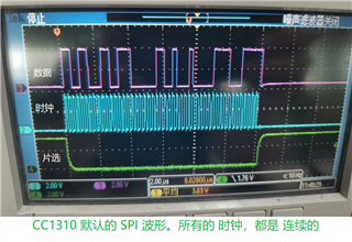
Call the SPI function library directly and modify the minDmaTransferSize to 1. If 5 bytes are written at a time, the oscilloscope shows 8*5 consecutive clock pulses with a CSN low (no interval, better SPI efficiency)

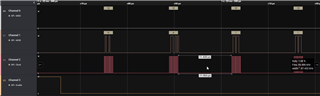
However, there is one device in the customer's actual circuit. When the device writes 5 bytes to it using SPI, it required to be separated by at least 2 every 8-tap clock before transmitting the next set of 8-tap clocks.

The customer would like to know how to increase this interval by modifying the SDK.

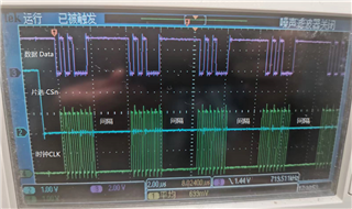
The oscilloscope waveform after implementation looks like the following picture:

Could you help check this case? Thanks.

Best Regards,

Cherry

  • Hi,

    May I know is there any update?

    Thanks and regards,

    Cherry

  • Hi,

    I have assigned somebody to look at the case

    Regards,

    Arthur

  • Hi Arthur,

    Thanks and the customer has posted the the default SPI waveform:

    The clock signal is continuous and has no interval. 

    Thanks and regards,

    Cherry

  • Hi Cherry, 

    This could be achieved by controlling the CS pin manually using a GPIO and sending one byte at a time using separate SPI_transfer. With this approach you don't need to modify the SPI driver code in the SDK.

    I unassigned the CSn pin in the SPI driver inside CC1310_LAUNCHXL.c:

    const SPICC26XXDMA_HWAttrsV1 spiCC26XXDMAHWAttrs[CC1310_LAUNCHXL_SPICOUNT] = {
        {
            .baseAddr           = SSI0_BASE,
            .intNum             = INT_SSI0_COMB,
            .intPriority        = ~0,
            .swiPriority        = 0,
            .powerMngrId        = PowerCC26XX_PERIPH_SSI0,
            .defaultTxBufValue  = 0xFF,
            .rxChannelBitMask   = 1<<UDMA_CHAN_SSI0_RX,
            .txChannelBitMask   = 1<<UDMA_CHAN_SSI0_TX,
            .mosiPin            = CC1310_LAUNCHXL_SPI0_MOSI,
            .misoPin            = CC1310_LAUNCHXL_SPI0_MISO,
            .clkPin             = CC1310_LAUNCHXL_SPI0_CLK,
            .csnPin             = PIN_UNASSIGNED, // <- csn pin controlled by software
            .minDmaTransferSize = 10
        },

    I tried out the following code in the spimaster example:

        /* Initialize master SPI transaction structure */
        txChar = masterTxBuffer[0];
        transaction.count = 1;
        transaction.txBuf = (void *) &txChar;
        transaction.rxBuf = (void *) masterRxBuffer;
    
        // deassert CS pin
        GPIO_write(Board_SPI_MASTER_CSn, 0);
        
        for (i = 0; i < SPI_MSG_LENGTH; i++){
            txChar = masterTxBuffer[i];
            transferOK = SPI_transfer(masterSpi, &transaction);
            if (!transferOK) {
                while(1){};
            }
        }
        
        // assert CS pin
        GPIO_write(Board_SPI_MASTER_CSn, 1);

    and obtained the following transaction on the logic analyzer:

    The interval between each byte transaction ends up being between 11 and 12us. It's hard to achieve tighter intervals between the bytes without modifying the SPI driver code. Would this work for the costumer?

    Regards,

    Fausto

  • Hi Fausto,

    Thanks for your support.

    The interval between each byte transaction ends up being between 11 and 12us

    11 to 12us is too slow for the customer and the actual circuit needs to use a rate of 4M for SPI. 

    to modify the SPI driver code in the SDK.

    Could you help point to the correspond file name?

    Thanks and regards,

    Cherry

  • Hi Cherry,

    The SPI driver code for CC1310 is located in <SDK>/source/ti/drivers/SPI.h and SPI.c. The device specific code is located in <SDK>/source/ti/drivers/spi/SPICC26XX.h and SPICC26XX.c . If the client wants to go even more low-level they will have to modify the ssi module in driverlib, located at <SDK>/source/ti/devices/cc13x0/driverlib/ssi.h and ssi.c

    Regards,

    Fausto

  • Hi Fausto,

    The customer has configured SPI for DMA mode,  clock 8M and SPI_POL0_PLA0. From the oscilloscope, we can know that two 8-bit intervals is 256 ns (approximately 2 taps 8M clock). Which parameter can be modified to increase the above interval to 4-tap 8M clock?

    If DMA mode is not used, the interval is 1.38us (approximately 11px 8M clock)  and it's still large. 8-bit interval 4 shots of 8M clock is required for the customer.

    The waveform refers to the spimaster's attempt code and uses an IO to generate the CSN signal. The SPI configuration is as follows:

       spiParams.transferMode = SPI_MODE_BLOCKING; //
       spiParams.dataSize = 8; // 8-bit data size
       spiParams.mode = SPI_MASTER; //SPI MASTER
       spiParams.frameFormat = SPI_POL0_PHA0;
       spiParams.bitRate = 8000000;

    Thanks and regards,

    Cherry

  • Hi,

    May I know is there any update on this?

    Thanks and regards,

    Cherry

  • Hi Cherry,

    When setting up the transfer in DMA mode the driver will not interfere with the SPI module once the transaction is started. the DMA HW module will automatically load bytes in the SPI TX FIFO and the SPI IP will transfer data as fast as it is allowed to run. Unfortunately there is no parameter or HW configuration of the SPI module allowing you to select the time interval between consecutive bytes (I couldn't find any setting in the TRM for the SSI module regarding this). The recorded time interval from your last post derive from the execution time of the code between one byte and the next. Therefore I don't think this use case is supported by our device. The customer will have to use either ~2 clock cycles (DMA transaction), ~11 clock cycles (non-DMA transaction) or implement a scaled down version of the SPI driver where they can have more accurate timing control.

    Regards,

    Fausto