This thread has been locked.

If you have a related question, please click the "Ask a related question" button in the top right corner. The newly created question will be automatically linked to this question.

CC1200: Optimum matching impedance

Part Number: CC1200

Dear Ti,

I have to develop a project with a CC1200. I need to customize it and i would like to know the measurement condition of the PA  and RX impedance. Reading the DS i found the parameters of the single ended PA and the Differential RX.

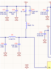
On your application note, i see that the PA is fed externally. Is the impedance at 868MHz of 35+j35 with the 10nH 15pF elements? Otherwise would it be enough an RF choke and a PI matching 60 to 50 ohm? 

See attached Fig 1

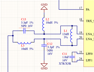
About the RX line i see a weird configuration of the DIFF to SE transformer.. is the L191 (15nH) to give a ground path to both side of the LNA? In that case the impedance will be slightly different..

I did some simulation, and i found what you can see in Fig 2. (Using a 2 ports model)

Waiting for your suggestion...

Fig1                                                          Fig 2


Thank you for your help,

Alex

  • The impedance is what the PA/ LNA should see into the external network. Meaning that if do a simulation, place a terminal (single ended for TX, differential for RX) at the position of the tx and rx pins. The impedance seen into the external network should be equal to what is stated in the datasheet. If you do simulation, you need to do that with ADS or similar to include the effects of the layout. 

  • Hi Alex,

    • To add to the post above, Section 9 of SWRA640F (CC13xx/CC26xx Hardware Configuration and PCB Design Considerations (Rev F)): https://www.ti.com/lit/swra640 provides addtional information on this process (which is the same although the target impedance is of course different for the CC1200).
    • L191 provides a path to GND for pin LNA_N, as you suggest. It forms part of the biasing network, along with L192. Otherwise LNA_N would be left floating. Normally the inductor would be a higher value, but in this design the inductor is incorporated into the matching network to resonate with the output capacitance of the device.
    • When designing the matching network it is important to account for the PCB parastics and component imperfections. Models of the passive components in the output path provided by the component manufacturers were used, as well as simulation of the PCB using Keysight ADS. The board was then tested and fine-tuned. Hence, you should target the impedance stated in the CC1200 datasheet for optimal performance.

    Regards,

    Zack