

Hi
i am using CC1101 as transciever.
output power level is very low though it is transmitting data. i checked it on hyperterminal.
So Receiver is not receiving any data.
can anyone pls tell me the reason for it???

This thread has been locked.
If you have a related question, please click the "Ask a related question" button in the top right corner. The newly created question will be automatically linked to this question.
Hi
i am using CC1101 as transciever.
output power level is very low though it is transmitting data. i checked it on hyperterminal.
So Receiver is not receiving any data.
can anyone pls tell me the reason for it???
You'll need to provide some more information such as what steps you are taking to get the radio to transmit, etc. before I can make any guesses as to what the problem is. Also, what platform are you using, i.e. what processor board and how is it connected to the CC1101.
Jim Noxon

i am attaching the circuit diagram.
Also can u tell me are there any settings that needs to be done if i am using a new ic of cc1101(first time)???
i am able to transmit data from controller to cc1101 but not getting any RF output from it.
Also if i give a 433Mhz signal from outside from rf signal generator, there is no output on SO line which goes to MISO further,
Plz help me out.
is the ic not working or are there any settings that i am not aware of while using cc1101 for the first time??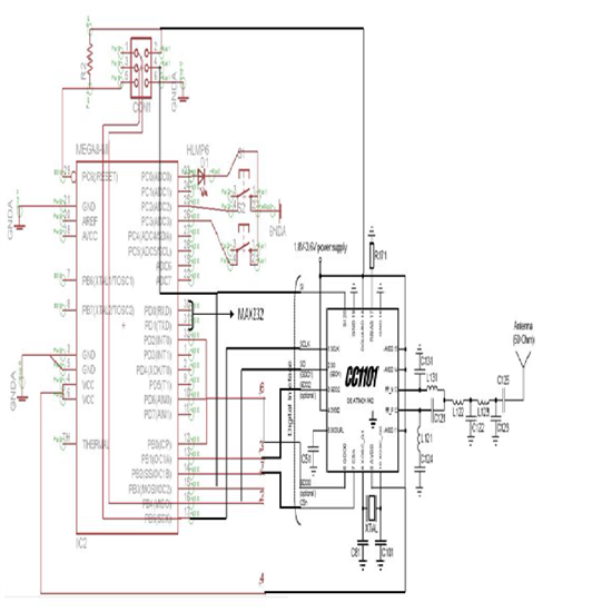

There are really only two reasons for the CC1101 to be pulling low current. 1) the ground pad under the chip is not properly connected, or 2) the chip has not received the appropriate commands to place it into either receive or transmit.
Many people are caught off guard by the ground connection under the part and this can be especially difficult to manage for prototype builds where assembly is done on a lab bench rather than with a reflow oven as on a manufacturing line. Not that it is impossible to solder on a lab bench, just that it can be difficult and if not practiced, may take several attempts to get it right.
The second issue is generally for people who are working with these radios for the first time. You can use the SmartRF Studio software (http://focus.ti.com/docs/toolsw/folders/print/smartrftm-studio.html) to help you create the appropriate register settings for the part to work in your application. Note that the part does not power up ready to transmit or receive, you must initialize it with the proper set of commands to make this happen not only the first time you power it on but every time you power it on.
Jim Noxon
hello sir
it started working yesterday and was properly receiving data packets till last night.
the die pad was not grounded as you said.
it drew current and buzzer sounded every time it received a data packets as per my code.
but it stopped working today morning :-(
now on receiving a data packet it sounds a buzzer just once and current drops to zero.
it sounds buzzer everytime we reset the ckt and then it doesnt.
It is possible your circuit originally was marginally working due to some debris or extra solder flux providing a workable ground connection. Perhaps moving the board or doing some other rework has dislodged whatever debris was letting it work and now you need to reflow the part.
Beyond this suggestion, I really cannot provide you much. Intermittent systems, especially if there are no code changes between working and not working, are always frustrating to debug. Persistence and creativity are about the only tools you have.
Good luck,
Jim Noxon
Sir it is finally working.
yes it was actually very frustrating.
Another doubt,Can cc1101 transmit and receive at the same time??
Actually i want that after transmitting a data packet,it should get a confirmation signal from receiver.
i incorporated the receiver function in transmitter code and called it after the data transmitting function.but it's not working.
current drawn by transmitter has reduced while it is drawing enough amount of current when it is only used as transmitter.
i am sending u the code for transmitter.
please go through it.
#include <io.h>
#include <sleep.h>
#include <delay.h>
#include <mega8.h>


 char data[20];
 int k;


void USART_Init(void)
{

    UBRRL = 25;                // sets 1Mhz, 2400bps, .2% error
    UCSRB = (1<<RXEN)|(1<<TXEN);        // Enable receiver and transmitter
    UCSRC = (1<<URSEL)|(1<<USBS)|(3<<UCSZ0);// Set frame format: 8data, 2stop bit
}


void USART_Transmit( char data )
{

    while ( !( UCSRA & (1<<UDRE)) )        // Wait for empty transmit buffer
    ;
    UDR = data;                // Put data into buffer, sends the data
}


unsigned char USART_Receive( void )
{

    while ( !(UCSRA & (1<<RXC)) )        // Wait for data to be received
    ;

    return UDR;                // Get and return received data from buffer
}


void Check_If_Done(char *str)
{

    while(*str)

        USART_Transmit(*str++);


}


void SPI_MasterInit(void)            //Initialize Atmega8 as master
{

    DDRB = (1<<DDB5)|(1<<DDB3)|(1<<DDB2);    // Set MOSI,SCK and SS\ output, all others input

    SPCR = (1<<SPE)|(1<<MSTR)|(1<<SPR0);    // Enable SPI, Master, set clock rate fck/16
}


void SPI_MasterTransmit(char cData)        //Transmit data on the SPI interface
{

    SPDR = cData;                // Start transmission

    while(!(SPSR & (1<<SPIF)))        // Wait for transmission complete
    ;
}

void CSn(int i)                    //Toggle CSn
{
    if(i==1)
    PORTB|=0x04;
    else
    PORTB&=0xFB;
}


void Write_RegConfig(char addr,char value)    //send register value of a particular register
{
    SPI_MasterTransmit(addr);
    SPI_MasterTransmit(value);
}


void SPI_MasterReceive(void)
        {
              char ReceivedValue[2];
           // SPI_MasterTransmit(0x3D);


             for(k=0;k<2;k++)
            {

                SPI_MasterTransmit(0x3D);

                ReceivedValue[k] = SPDR;

            }

            if((ReceivedValue[0]=='h') & (ReceivedValue[1]=='i'))
            {
              Check_If_Done(ReceivedValue);
                PORTC=0x01;
                    }


               }


void Full_RegConfig(void)            //for full register configuration using BURST access
{
    CSn(0);
    while(PORTB.4==1){}

    SPI_MasterTransmit(0x3E);        //address for patable access
    SPI_MasterTransmit(0xC0);        //patable for PA power control settings

    SPI_MasterTransmit(0x40);        //burst transfer 1st address

    SPI_MasterTransmit(0x29);        //data written at register 0x00
    SPI_MasterTransmit(0x2E);        //data written at register 0x01
    SPI_MasterTransmit(0x06);        //data written at register 0x02
    SPI_MasterTransmit(0x47);        //data written at register 0x03
    SPI_MasterTransmit(0xD3);        //data written at register 0x04
    SPI_MasterTransmit(0x91);        //data written at register 0x05
    SPI_MasterTransmit(0x3D);        //data written at register 0x06
    SPI_MasterTransmit(0x00);        //data written at register 0x07 EARLIER 04
    SPI_MasterTransmit(0x01);        //data written at register 0x08 EARLIER 05
    SPI_MasterTransmit(0x00);        //data written at register 0x09
    SPI_MasterTransmit(0x00);        //data written at register 0x0A
    SPI_MasterTransmit(0x06);        //data written at register 0x0B
    SPI_MasterTransmit(0x00);        //data written at register 0x0C
    SPI_MasterTransmit(0x10);        //data written at register 0x0D
    SPI_MasterTransmit(0x09);        //data written at register 0x0E EARLIER A7 866
    SPI_MasterTransmit(0x7B);        //data written at register 0x0F EARLIER 62 866
    SPI_MasterTransmit(0xF5);        //data written at register 0x10    CA
    SPI_MasterTransmit(0x75);        //data written at register 0x11    EARLIER 83 866
    SPI_MasterTransmit(0x03);        //data written at register 0x12    13
    SPI_MasterTransmit(0x22);        //data written at register 0x13
    SPI_MasterTransmit(0xE5);        //data written at register 0x14    EARLIER F8 866
    SPI_MasterTransmit(0x14);        //data written at register 0x15 EARLIER 15 866
    SPI_MasterTransmit(0x07);        //data written at register 0x16
    SPI_MasterTransmit(0x30);        //data written at register 0x17
    SPI_MasterTransmit(0x18);        //data written at register 0x18
    SPI_MasterTransmit(0x16);        //data written at register 0x19
    SPI_MasterTransmit(0x6C);        //data written at register 0x1A
    SPI_MasterTransmit(0x03);        //data written at register 0x1B
    SPI_MasterTransmit(0x40);        //data written at register 0x1C
    SPI_MasterTransmit(0x91);        //data written at register 0x1D
    SPI_MasterTransmit(0x87);        //data written at register 0x1E
    SPI_MasterTransmit(0x6B);        //data written at register 0x1F
    SPI_MasterTransmit(0xF8);        //data written at register 0x20
    SPI_MasterTransmit(0x56);        //data written at register 0x21
    SPI_MasterTransmit(0x10);        //data written at register 0x22
    SPI_MasterTransmit(0xE9);        //data written at register 0x23
    SPI_MasterTransmit(0x2A);        //data written at register 0x24
    SPI_MasterTransmit(0x00);        //data written at register 0x25
    SPI_MasterTransmit(0x1F);        //data written at register 0x26
    SPI_MasterTransmit(0x41);        //data written at register 0x27
    SPI_MasterTransmit(0x00);        //data written at register 0x28
    SPI_MasterTransmit(0x59);        //data written at register 0x29
    SPI_MasterTransmit(0x7F);        //data written at register 0x2A
    SPI_MasterTransmit(0x3F);        //data written at register 0x2B
    SPI_MasterTransmit(0x81);        //data written at register 0x2C
    SPI_MasterTransmit(0x35);        //data written at register 0x2D
    SPI_MasterTransmit(0x09);        //data written at register 0x2E

    CSn(1);

}


void SimpleReceive(void)
        {

            CSn(0);
            while(PINB.4==1){}

            SPI_MasterTransmit(0x34);        //SRX STROBE


           // while(PINB.0==0){}
            //Check_If_Done(sync);

           // while(PINB.0==1){}
           // Check_If_Done(pkt);


            SPI_MasterTransmit(0xFF);        //BURST READ RXFIFO

            SPI_MasterReceive();
            CSn(1);

            }


void TransmitUDPacket(char *str)
{

    char sync[] = "SYNC TX";

    char pkt[] = "PACKET TX";

    CSn(0);
    while(PORTB.4==1){}

    SPI_MasterTransmit(0x35);

    SPI_MasterTransmit(0x7F);        //write TXFIFO

    while(*str)
        SPI_MasterTransmit(*str++);


       SimpleReceive();

   CSn(1);

}
// Timer1 overflow interrupt service routine
interrupt [TIM1_OVF] void timer1_ovf_isr(void)
{
// Reinitialize Timer1 value
TCNT1H=0xF85D >> 8;
TCNT1L=0xF85D & 0xff;
// Place your code here
delay_ms(1000);
}


void main()
{

    char done[] = "Done";

    char start[] = "Start";


    // Timer/Counter 1 initialization
// Clock source: System Clock
// Clock value: 0.977 kHz
// Mode: Normal top=FFFFh
// OC1A output: Discon.
// OC1B output: Discon.
// Noise Canceler: Off
// Input Capture on Falling Edge
// Timer1 Overflow Interrupt: On
// Input Capture Interrupt: Off
// Compare A Match Interrupt: Off
// Compare B Match Interrupt: Off
TCCR1A=0x00;
TCCR1B=0x05;
TCNT1H=0xF8;
TCNT1L=0x5D;
ICR1H=0x00;
ICR1L=0x00;
OCR1AH=0x00;
OCR1AL=0x00;
OCR1BH=0x00;
OCR1BL=0x00;

// Timer(s)/Counter(s) Interrupt(s) initialization
TIMSK=0x04;


//#asm("sei")
 SFIOR=(0<<PUD);
  //  DDRC = (0<<DDC3)|(0<<DDC2)|(1<<DDC0);
   // PORTC = (1<<PC3)|(1<<PC2)|(0<<PC0);
     DDRC=0x01;

    SPI_MasterInit();            //initialize SPI

    USART_Init();                //initialize USART

    Check_If_Done(start);            //print Start

    Full_RegConfig();            //CC1101 configured

    Check_If_Done(done);            //print Done

        data[0]=9;
        data[1]='a';
        data[2]='b';
        data[3]='c';
        data[4]='d';
        data[5]='e';
        data[6]='f';
        data[7]='g';
        data[8]='h';
        data[9]='K';
        data[10]='\0';


    while(1)
   {

       #asm("sei")
      sleep_enable();
      idle();
      data[9]='y';
         PORTC=0x01;
      // delay_ms(100);
        TransmitUDPacket(data);

      Check_If_Done(data);
      PORTC=0x00;

//        TransmitUDPacket(data);

    }

  //  return 0;
}
Jaspreet Kaur said:yes it was actually very frustrating.
I'm sure there are plenty of people on the forum who would be happy to start up a support group for intermittent problems. I certainly would have plenty of stories to relate! :-)
As for your code, I think you need to issue an SIDLE strobe to the radio before you move to the RX state. EIther that or make sure you wait for the radio to move to IDLE state before you issue the SRX command. I would suggest just issuing the SIDLE command as that will alleviate the need to check for other invalid states due to a failed transmission but then again you may not receive the acknowledge packet if your transmission never went out.
It is always the question of how much intelligence to put into the code vs how much usefulness it will provide you. Since you will need to manage having not received an acknowledgment packet anyway, does it really matter why it was not received? Other than for your own comfort level or to understand the actual failure, simply managing the missing acknowledgement should suffice.
Jim Noxon
Sir i am not able to switch between rx and tx modes.
In receiver side, i issued sidle,sfrx strobes and after a delay of 50ms i issued scal strobe.
these strobes were issued before transmitter function.
there are no results ,buzzer sounds once and then nothing happens unless a reset o
        #include <avr/io.h>
        #include <util/delay.h>
		#define F_CPU 1000000

        void USART_Init(void)
        {

            UBRRL = 25;				// sets 1Mhz, 2400bps, .2% error
            UCSRB = (1<<RXEN)|(1<<TXEN);		// Enable receiver and transmitter
            UCSRC = (1<<URSEL)|(1<<USBS)|(3<<UCSZ0);// Set frame format: 8data, 2stop bit

        }


        void USART_Transmit( char data )
        {

            while ( !( UCSRA & (1<<UDRE)) )		// Wait for empty transmit buffer
            ;
            UDR = data;				// Put data into buffer, sends the data
        }


        void Check_If_Done(char *str)
        {

            while(*str)

                USART_Transmit(*str++);


        }


        void SPI_MasterInit(void)			//Initialize Atmega8 as master
        {

            DDRB = (1<<DDB5)|(1<<DDB3)|(1<<DDB2);	// Set MOSI,SCK and SS\ output, all others input

            SPCR = (1<<SPE)|(1<<MSTR)|(1<<SPR0);	// Enable SPI, Master, set clock rate fck/16
        }


        void SPI_MasterTransmit(char cData)		//Transmit data on the SPI interface
        {

            SPDR = cData;				// Start transmission

            while(!(SPSR & (1<<SPIF)))		// Wait for transmission complete
            ;
        }


		void TransmitUDPacket(char *str)
		{

    char sync[] = "SYNC TX";

    char pkt[] = "PACKET TX";

    //CSn(0);
  //  while(bit_is_set(PINB,4)){}
     SPI_MasterTransmit(0x36);     //idle mode
	 SPI_MasterTransmit(0x3A);     //rx flush

	  _delay_ms(50);

	 SPI_MasterTransmit(0x33);	   // scal strobe


    SPI_MasterTransmit(0x35);
    SPI_MasterTransmit(0x7F);        //write TXFIFO

    while(*str)
        SPI_MasterTransmit(*str++);


		SPI_MasterTransmit(0x3B);

   /* while(bit_is_clear(PINB,0))
    {
    //PORTC=0x01; //set PC0 high
    //delay_ms(100);

    }
    Check_If_Done(sync);            //print SYNC TX when sync transmission gets completed

    while(bit_is_set(PINB,0))
    {
    //PORTC=0x00;
    }
    Check_If_Done(pkt);            //print PACKET TX when packet transmission gets completed
     //*/

    //CSn(1);

}


        void SPI_MasterReceive(void)
        {
            char RegValue, i;
            char ReceivedValue[11];
			unsigned char c;
			float RSSI_dec;
			float RSSI_dBm;
			char trans[3];
			trans[0]= 'h';
			trans[1]= 'i';
			trans[2]= '\0';

            char on[]="ON";
            char off[]="OFF";

            SPI_MasterTransmit(0x3D);

            RegValue = SPDR;

            USART_Transmit(RegValue);

            for(i=0; i<11; i++)
            {

                SPI_MasterTransmit(0x3D);

                ReceivedValue[i] = SPDR;

            }

            if((ReceivedValue[0]=='a') & (ReceivedValue[1]=='b') & (ReceivedValue[2]=='c') & (ReceivedValue[3]=='d') & (ReceivedValue[4]=='e') & (ReceivedValue[5]=='f') & (ReceivedValue[6]=='g') & (ReceivedValue[7]=='h'))
            {
                if((ReceivedValue[8]=='y'))

                {
                   PORTC|=((1<<PC0)|(1<<PC1)|(1<<PC2));
				   Check_If_Done(ReceivedValue);
                        _delay_ms(250);
					TransmitUDPacket(trans);
					Check_If_Done(trans);
                    PORTC&=~(1<<PC0);


				}
				/*c=ReceivedValue[9];
				RSSI_dec=(float)c;

				if(RSSI_dec>= 128)
				RSSI_dBm =((RSSI_dec - 256)/2 - 74);
				else
				RSSI_dBm =((RSSI_dec)/2 - 74);

				 if(RSSI_dBm<(-107))
				{
				PORTC|=(1<<PC0);
				 _delay_ms(1000);
                PORTC&=~(1<<PC0);
					}


			/*	if (RSSI_dec<190)
				{
				PORTC|=(1<<PC0);
				 _delay_ms(1000);
                PORTC&=~(1<<PC0);
				}


                /*else if((ReceivedValue[8]=='n'))
                {
                    PORTC&=~((1<<PC1)|(1<<PC2));
                    PORTC|=(1<<PC0);
                        _delay_ms(1000);
                    PORTC&=~(1<<PC0);
                    Check_If_Done(off);*/
                }
            }


        void CSn(int i)					//Toggle CSn
        {
            if(i==1)
            PORTB|=0x04;
            else
            PORTB&=0xFB;
        }


        void Write_RegConfig(char addr,char value)	//send register value of a particular register
        {
            SPI_MasterTransmit(addr);
            SPI_MasterTransmit(value);
        }


        void Full_RegConfig(void)			//for full register configuration using BURST access
        {
            CSn(0);
            while(bit_is_set(PINB,4)){}

            SPI_MasterTransmit(0x3E);		//address for patable access
            SPI_MasterTransmit(0xC0);		//patable for PA power control settings

            SPI_MasterTransmit(0x40);		//burst transfer 1st address

            SPI_MasterTransmit(0x29);		//data written at register 0x00
            SPI_MasterTransmit(0x2E);		//data written at register 0x01
            SPI_MasterTransmit(0x06);		//data written at register 0x02
            SPI_MasterTransmit(0x47);		//data written at register 0x03
            SPI_MasterTransmit(0xD3);		//data written at register 0x04
            SPI_MasterTransmit(0x91);		//data written at register 0x05
            SPI_MasterTransmit(0x3D);		//data written at register 0x06
            SPI_MasterTransmit(0x04);		//data written at register 0x07 EARLIER 04
            SPI_MasterTransmit(0x01);		//data written at register 0x08 EARLIER 05
            SPI_MasterTransmit(0x00);		//data written at register 0x09
            SPI_MasterTransmit(0x00);		//data written at register 0x0A
            SPI_MasterTransmit(0x06);		//data written at register 0x0B
            SPI_MasterTransmit(0x00);		//data written at register 0x0C
            SPI_MasterTransmit(0x10);		//data written at register 0x0D
            SPI_MasterTransmit(0x09);		//data written at register 0x0E EARLIER A7 866
            SPI_MasterTransmit(0x7B);		//data written at register 0x0F EARLIER 62 866
            SPI_MasterTransmit(0xF5);		//data written at register 0x10	CA
            SPI_MasterTransmit(0x75);		//data written at register 0x11	EARLIER 83 866
            SPI_MasterTransmit(0x03);		//data written at register 0x12	13
            SPI_MasterTransmit(0x22);		//data written at register 0x13
            SPI_MasterTransmit(0xE5);		//data written at register 0x14	EARLIER F8 866
            SPI_MasterTransmit(0x14);		//data written at register 0x15 EARLIER 15 866
            SPI_MasterTransmit(0x07);		//data written at register 0x16
            SPI_MasterTransmit(0x30);		//data written at register 0x17
            SPI_MasterTransmit(0x18);		//data written at register 0x18
            SPI_MasterTransmit(0x16);		//data written at register 0x19
            SPI_MasterTransmit(0x6C);		//data written at register 0x1A
            SPI_MasterTransmit(0x03);		//data written at register 0x1B
            SPI_MasterTransmit(0x40);		//data written at register 0x1C
            SPI_MasterTransmit(0x91);		//data written at register 0x1D
            SPI_MasterTransmit(0x87);		//data written at register 0x1E
            SPI_MasterTransmit(0x6B);		//data written at register 0x1F
            SPI_MasterTransmit(0xF8);		//data written at register 0x20
            SPI_MasterTransmit(0x56);		//data written at register 0x21
            SPI_MasterTransmit(0x10);		//data written at register 0x22
            SPI_MasterTransmit(0xE9);		//data written at register 0x23
            SPI_MasterTransmit(0x2A);		//data written at register 0x24
            SPI_MasterTransmit(0x00);		//data written at register 0x25
            SPI_MasterTransmit(0x1F);		//data written at register 0x26
            SPI_MasterTransmit(0x41);		//data written at register 0x27
            SPI_MasterTransmit(0x00);		//data written at register 0x28
            SPI_MasterTransmit(0x59);		//data written at register 0x29
            SPI_MasterTransmit(0x7F);		//data written at register 0x2A
            SPI_MasterTransmit(0x3F);		//data written at register 0x2B
            SPI_MasterTransmit(0x81);		//data written at register 0x2C
            SPI_MasterTransmit(0x35);		//data written at register 0x2D
            SPI_MasterTransmit(0x09);		//data written at register 0x2E

            CSn(1);

        }


        void SimpleReceive(void)
        {
			//char RSSI_value;

            char sync[] = "SYNC TX";

            char pkt[] = "PACKET TX";

            while(1)
            {

            CSn(0);
            //while(bit_is_set(PINB,4)){}
			 _delay_ms(100);
            SPI_MasterTransmit(0x34);		//SRX STROBE


            while(bit_is_clear(PINB,0)){}
            Check_If_Done(sync);

            while(bit_is_set(PINB,0)){}
            Check_If_Done(pkt);


            SPI_MasterTransmit(0xFF);		//BURST READ RXFIFO

            SPI_MasterReceive();

			//SPI_MasterTransmit(0xF4);
			//RSSI_value=SPDR;
			//USART_Transmit(RSSI_value);


            CSn(1);

            }

        }


        int main()
        {

            char done[] = "Done";

            char start[] = "Start";

            DDRC =(1<<DDC2)|(1<<DDC1)|(1<<DDC0);	// 0 for Buzzer, 1 for LED, 2 for Relay
            PORTC =(1<<PC2)|(0<<PC1)|(0<<PC0);

            SPI_MasterInit();

            USART_Init();


            Check_If_Done(start);

            Full_RegConfig();			//CC1101 configured

            Check_If_Done(done);

            SimpleReceive();

            return 0;
        }
i am attaching the receiver code.please go through it. earlier i gave u the transmitter code.
Hello Sir,
I am facing a peculiar problem.
CC1101 is transmitting well but not able to receive the data packet.
The codes are well tested.Can it be a hardware problem???
Sure, it can be hardware. I recently debugged an issue where the 56k bias resistor was replaced with a 56 ohm resistor. This caused an asymmetric response between transmit and receive, the distance in receive was about 2 orders of magnitude shorter than in transmit. That's not to say this is your problem but just to show there can be real hardware issues that cause asymmetric operation of the RF path.
Usually when people have these types of problems it generally is a configuration issue. When you say the code is well tested, how do you know that. Does it run on one of the EM boards properly but not on yours?
I'll need a bit more information to be able to help you much.
Jim Noxon
Yes sir it did run on the similar boards...but now when i have the new pcb with me..it's not receiving but it is doing the transmitting part....
That it is transmitting, grounding of the die pad won't be a problem i guess...
What could be the problem then???
There's really no way for me to tell exactly. My suggestion is to make sure all the components (bias resistor, bypass capacitors, etc.) match what the reference designs use. Also make sure the RF path is using good quality components to minimize tolerance issues. Finally, does your layout conform to one of the reference designs especially with respect to the bypass capacitors and power line traces. The last item can have a significant effect on generation of asymmetric operation as different power pins are more closely associated with RX and TX blocks within the parts.
Jim Noxon
Hi Jim
Gin here, from IdentiTag, South Africa
I hope you could possibly give me some advice
We recently had some issues using the CC1101 in our manufacturing process.
A set of boards were processed using a proper solder stencil, pick and place, and re-flow oven.
A lead-free paste and oven profile was used.
Approximately 40% of the units failed on main test, due to the boards not being able to produce an RF carrier.
The following was confirmed for all affected boards:
I do not think this was MSD or ESD related, as the same identical symptoms were seen over a fair number of units.
Surely the symptoms would be more random if the ICs were damaged by static, or mechanical strain?
Thus far all I can imagine is that perhaps a poor centre pad connection, and enabling the RF PA, somehow damaged the chips.
Our SMD production manager mentioned that we do run a slightly cooler re-flow profile than usual.
This might explain a possible poor re-flow on the centre pad, due to it being effectively heatsinked by the ground plane it is connected to.
Have you had any similar complaints / feedback from other users?
Yes I have. Lead free solders tend to have a higher melting point and therefore need a higher temperature profile during reflow. This carries the potential to damage the part and as you have seen, lowering the temperature profile can lead to incomplete reflow. If replacing the part fixes the problem then it appears the RF path is valid so we don't need to investigate that path. I would suggest you X-ray the modules that are failing and compare them with X-rays of modules which are passing.
Another option is the solder past mask is too large and you are getting shorts from the ground pad to other pins (such as the RF pins) on the part causing failure. This usually can be determined if the pass/fail criteria have a very large gap whereas poor ground pad connections do to failed reflow usually show a more distributed failure of output power.
I have also heard of some cases where older reflow equipment had larger than acceptable gradients within the oven and the area where the radio was at failed purely due to these gradients. This is a long shot but you can check with your CM to see how old the equipment being used is. You can use a blank board with several different temperature test strips placed on it at several locations to validate an even reflow process if there is any question.
Another option is if the via's under the part trap air or more importantly gas from the flux as it boils away. This can lift the part or create large voids under the part. Eliminating the center via can sometimes circumvent this failure. Another option would be to specify these vias be filled during the board fabrication process.
Unfortunately there is no magic answer for such problems. This is usually more of a Sherlock Holmes type of process where you eliminate all that is not failing and you are finally left with the real failure. Regrettably this is usually a long and drawn out process. Keep us informed of anything you find as it may trigger some old memory that I have yet to conjure up.
Best of luck,
Jim Noxon
Hi Jim
Our oven is indeed old - a four stage from the 90's.
I know that our production manager has been looking at running a thermal data-logger through the oven, to get a better idea of what it's actually doing.
We should have an answer on that hopefully soon.
I'm quite confident that we're not getting shorts.
I tested for continuity along the pins of three problem units, nothing suspicious was found.
As for Vias, I have four vias in the ground pad, 0.3mm drill, tented on the bottom side.
I'm quite certain that we could specify these to be filled by our manufacturer.
Thank you for your advice, it is very much appreciated.
I shall let you know as soon as we have resolved this problem.
Kind regards
Gin