This thread has been locked.
If you have a related question, please click the "Ask a related question" button in the top right corner. The newly created question will be automatically linked to this question.
Hi,
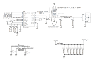
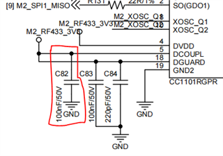
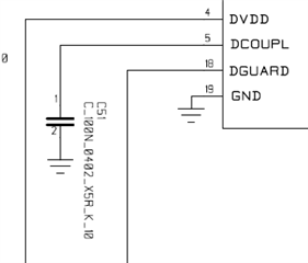
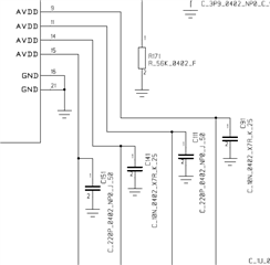
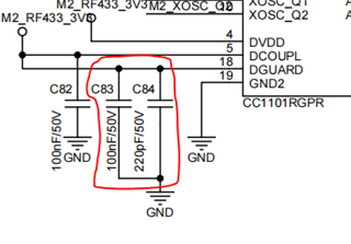
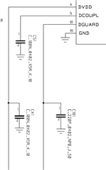
Please kindly review the schematic diagram that the CC1101 has no TX and RX signal,
The waveform of the power supply during transmission is normal, with a floating range of<30mV. Ripple<20mV, thanks.
Hi Zhang,
The most critical error I found is that DCOUPL should not be connected to VDD.
The only connection to this pin should be the 100nF decoupling capacitor. Image below from reference design.
I also noticed that the decoupling capacitors for AVDD are different than the reference design. In the reference design it uses 220pF and 20nF capacitors depending on the pin, while in your design, it seems that 100 nF capacitors were used for all of the AVDD pins.
Finally, the DGUARD pin should only have a 220pF capacitor.
Image below from reference design.
You can find the CC1101EM reference design for 433 MHz here: www.ti.com/.../swrr046
Hi,
This is the pilot production and the fault rate is 27%(8/30) , we have no idea if we don't change the PIN5 design and is there any other improve for this design, thanks?
Hi Zhang,
PIN5 (DCOUPL) needs to be disconnected from 3.3 V in the design. This pin is used only to connect the decoupling capacitor for the internal 1.6 - 2.0 V digital power supply. In your current design you are shorting 3.3 V to the internal power supply.
You are also exceeding the maximum voltage allowed on the DCOUPL pin.
Images above from the datasheet: https://www.ti.com/lit/ds/symlink/cc1101.pdf
Hi,
Because we have pilot production the error design about 100boards, so please advise if we can do something on the current boards, thanks.
Hi,
For testing, you may be able to cut the trace the connects DCOUPL to 3.3 V and just keep DCOUPL connected to the decoupling capacitor. If you can do this will depend on the board layout.