Because of the Thanksgiving holiday in the U.S., TI E2E™ design support forum responses may be delayed from November 25 through December 2. Thank you for your patience.

This thread has been locked.

If you have a related question, please click the "Ask a related question" button in the top right corner. The newly created question will be automatically linked to this question.

CC1350: Noise in DCDC inductor

Part Number: CC1350

Hello, I have an application where we are seeing a lot of additional noise in the DCDC path of the 1350 chip. It causes up to a doubling of the standby current of the device, which is a severe hit on our battery life. We are currently failing the devices with this issue during production testing, so it would be great with some pointers to how we can solve this.

I am suspecting an issue with the inductor layout or the inductor selection. In this design we're using Taiyo Yuden CBMF1608T100K, which is an unshielded wirewound inductor, with this layout:
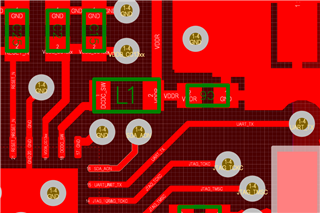
I have very limited experience with the DCDC design, so I'm looking for some pointers. I had a look at the design guideline https://www.ti.com/lit/an/swra640g/swra640g.pdf but didn't find the DCDC regulator part very helpful. The C6 capacitor power route is a bit unfortunate, if that could cause this issue?

Other notes:

  • The issue affects about 2% of our tested devices.
  • Issue seems to be specific to the CC1350-device: Swapping 1350 on a failed PCBA to a passed PCBA will still fail the same CC1350 component, and conversely the other CC1350 will still pass.
  • Placing a piece of metal (I used an insulated screwdriver tip) between the DCDC inductor and the CC1350 chip will remove the noise, and reduce the standby current down to the acceptable level.
  • Swapping the inductor to a shielded multilayer variant reduces the noise (and standby current) considerably. I tried Murata LQM18DN100M70L for example

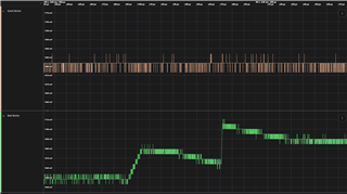
I captured the voltage on VDDR on both devices (powered from the same battery pack), and the "bad device" looks a lot more noisy. Again, I'm not sure what I'm looking for, so I'll be happy to capture more data if needed.
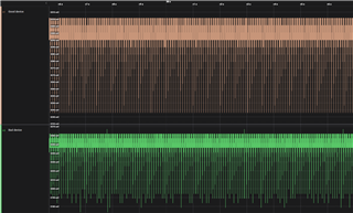
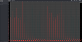
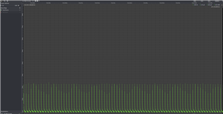
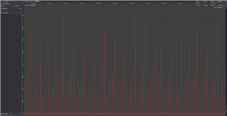
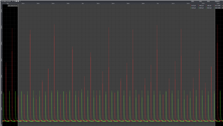
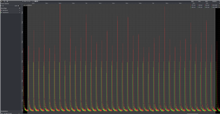
The issue is a lot more apparent in the current draw, so I'll attach some plots of that too: ("good" device in green / "bad" device in red)
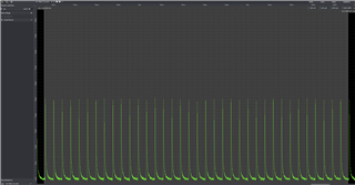
Any pointers are greatly appreciated, thanks!

  • DCDC performance is highly dependent on the inductor used. I would use the TDK part used in the ref designs. I believe it's a lot of app notes from different vendors on general DCDC usage that could cover this in more detail than SWRA640.

  • Hi Olav,

    Could you test using the internal LDO to verify if a good and bad device draw the same current using the LDO? To test this you need to remove the inductor and modify the CCFG file to use the LDO.

    In the voltage plots you mentioned that this are for VDDR, however looking at the voltage level this seem to be for VDDS. VDDR voltage should be around 1.7 V.

  • Hi Diego,

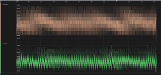
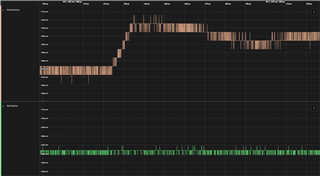
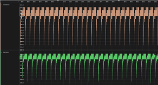
    You are of course correct and I measured VDDS instead, apologies.. Here are the actual measurements of VDDR in DCDC mode:

    Smaller timescale:

    I soldered off the inductors and disabled the DCDC, and they also draw different currents in LDO mode (3.48uA on the bad device, versus 2.72 on the good one). I'll attach the current draw plots as before (good in green, bad in red), let me know if there is anything else I should capture.

    Together:

    Individual:

    Thank you

  • Hi Olav,

    Would it be possible to get plots of VDDR with a higher sample rate?

    in your test code are you using any peripherals or setting certain pins as input or outputs? Or are the devices just going into standby?

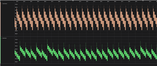
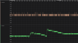
  • This is the maximum sample rate of my oscilloscope (50 MS/s) at a smaller timescale. I'm assuming the points where it "jumps" are the interesting parts.

    The good device looks pretty much like this every time:

    While the bad device is a mix between these smaller and larger jumps:

    I will attach an export of 250ms data from both channels if you want to poke around: analog.csv

    I'm instrumenting a production test image, so the I2C and GPIO peripherals are enabled prior to going to standby (I2C clock is disabled after use though). At standby I have two pins in output and one input. I didn't think to disable it since I can move the cc1350 chip between different PCBAs and see the same behavior, but I will make a test program that just goes to standby and see if it makes a difference.

  • Seeing that you also have higher current consumption with the internal LDO, it makes me believe that there may be peripheral or gpio that causes the higher current consumption. Check that pins that have pull ups or pull downs are set to a state that don't draw current and output pins are not sourcing current to another component. Please let us know the results with the program that just goes into standby.

  • That makes sense, but I am not able to remove the noise nor the higher current consumption. I tried a couple things to try and pin down the cause:

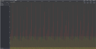
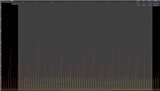
    1. Made a test program that simply enters standby. No peripherals enabled, GPIOs untouched. Both devices are still in LDO mode. Good device in green, bad in red:

    Quite a bit higher average current drain, probably caused by some active components that need to be put in reset.

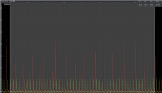
    2. Soldered off all other active external components, including pull-resistors on GPIOs, to exclude interference from them. This reduces the standby currents again, but the bad device is still visibly different from the good one, and draws more current. Very similar current drains to the production test program I used above:

    3. Modified the test program to enable the GPIO peripheral and drive all pins low (just to make sure they are not floating). Very little difference

  • What  is new/ different in this design vs what you done before with CC1350? 

  • Hi Olav,

    Could you desolder the bad device and measure resistance of each pin to ground and post the results?

  • The design is quite similar to another design we have, where we have not observed this error mode. Relevant differences:

    1. DCDC inductor is rotated 90 degress (same inductor)
    2. DCDC bulk cap on VDDR (C6 in the OP image) is significantly larger (22uF in this design, 2.2uF in previous)
      • This cap is also placed outside the power path in this design, as mentioned in the OP

    Since we're observing the noisy condition also in LDO mode, I tried to reduce the bulk capacitance near the DCDC inductor (C6 again). Reducing this to 2.2uF seems to remove the noisy behavior. This also removed the noise with the DCDC enabled again. I therefore tried to play with the ccfg option SET_CCFG_MODE_CONF_VDDR_CAP, but had no luck replicating the workaround with the 22uF cap. Since 22uF is used in the reference design, I'm not comfortable with reducing it without knowing the root cause of the noise.

  • Hi Diego,

    I can do that, I assume you meant the chip (and not on the PCBA). This is the RSM variant, and I used pin 3 as the ground connection. NC just means my multimeter was unable to measure a connection at all

    # Name Resistance [ohm]
    1 RF_P 2.1M
    2 RF_N 2.1M
    3 VSS -
    4 RX_TX 0.8M
    5 X32K_Q1 0.98M
    6 X32K_Q2 2.4M
    7 VSS 6.4
    8 DIO_0 NC
    9 DIO_1 NC
    10 DIO_2 NC
    11 VDDS2 NC
    12 DCOUPL 1.0M
    13 JTAG_TMSC NC
    14 JTAG_TCKC NC
    15 DIO_3 NC
    16 DIO_4 NC
    17 VSS 6.6
    18 DCDC_SW 1.5M
    19 VDDS_DCDC 1.8M
    20 VSS 6.4
    21 RESET_N 1.6M
    22 DIO_5 1.1M
    23 DIO_6 1.3M
    24 DIO_7 1.3M
    25 DIO_8 1.0M
    26 DIO_9 1.3M
    27 VDDS 0.9M
    28 VDDR 1.3M
    29 VSS 7.5
    30 X24M_N 0.7M
    31 X24M_P 0.8M
    32 VDDR_RF 1.8M
    33 PAD 10M
  • Hi Olav,

    Could you verify the measurement for the pins you mention that you didn't get a measurement (NC)? You should be able to read some resistance on those pins. Try with different VSS pins.

  • I had to get some new probes and use a different multimeter, but here I have repeated the measurements on all the pins:

    # Name R_CHIP [ohm]
    1 RF_P 1.8M
    2 RF_N 1.8M
    3 VSS 5.3
    4 RX_TX 88k
    5 X32K_Q1 103k
    6 X32K_Q2 2.6M
    7 VSS -
    8 DIO_0 16.9M
    9 DIO_1 16.9M
    10 DIO_2 16.9M
    11 VDDS2 15.1M
    12 DCOUPL 119k
    13 JTAG_TMSC 16.9M
    14 JTAG_TCKC 16.9M
    15 DIO_3 16.9M
    16 DIO_4 16.9M
    17 VSS 5.4
    18 DCDC_SW 131k
    19 VDDS_DCDC 1.4M
    20 VSS 5.4
    21 RESET_N 1.8M
    22 DIO_5 1.3M
    23 DIO_6 1.3M
    24 DIO_7 1.2M
    25 DIO_8 1.1M
    26 DIO_9 1.2M
    27 VDDS 220k
    28 VDDR 97k
    29 VSS 6.7
    30 X24M_N 72k
    31 X24M_P 92k
    32 VDDR_RF 1.4M
    33 PAD 1.7M

    I tried both pin 7 and pin 29 as VSS this time around, and got similar results, hope this is better.

    Edit: I seem to have pressed the resolve-button by accident, sorry, I can't seem to undo that..

  • Resistance on some of the pins seems low. Could you please do the same measurements on a good device that you have?

  • Absolutely, repeated measurements with two good devices, and another bad one.

    # Name Bad Device 1 Bad Device 2 Good Device 1 Good Device 2
    1 RF_P 1.8M 92.4k 92.8k 81k
    2 RF_N 1.8M 92.6k 92.9k 81k
    3 VSS 5.3 6.5 6.7 6.7
    4 RX_TX 88k 101k 101k 95k
    5 X32K_Q1 103k 124k 124k 114k
    6 X32K_Q2 2.6M 46.7k 124k 114k
    7 VSS - 2.9 3.3 3
    8 DIO_0 16.9M 16.7M 17.4M 17M
    9 DIO_1 16.9M 16.8M 17.3M 17M
    10 DIO_2 16.9M 16.8M 17.4M 17M
    11 VDDS2 15.1M 14.6M 15.4M 15M
    12 DCOUPL 119k 116k 138K 134k
    13 JTAG_TMSC 16.9M 16.4M 17.2M 17M
    14 JTAG_TCKC 16.9M 16.5M 17.3M 17M
    15 DIO_3 16.9M 16.4M 17.2M 17M
    16 DIO_4 16.9M 16.4M 17.2M 17M
    17 VSS 5.4 2.9 3 3
    18 DCDC_SW 131k 126k 1.8M 1.4M
    19 VDDS_DCDC 1.4M 1.4M 1.4M 1.5M
    20 VSS 5.4 3 3.4 3
    21 RESET_N 1.8M 1.8M 1.4M 1.8M
    22 DIO_5 1.3M 1.1M 1.2M 1.1M
    23 DIO_6 1.3M 1.2M 1.1M 1.1M
    24 DIO_7 1.2M 1.1M 1.1M 1.1M
    25 DIO_8 1.1M 1.1M 1.7M 1.1M
    26 DIO_9 1.2M 1.2M 1.1M 2M
    27 VDDS 220k 117k 160k 115k
    28 VDDR 97k 94k 130k 150k
    29 VSS 6.7 2.9 6.7 -
    30 X24M_N 72k 90k 90k 83k
    31 X24M_P 92k 100k 100k 78k
    32 VDDR_RF 1.4M 62k 62k 50k
    33 PAD 1.7M 1.8M 1.9M 1.2M
  • Small update, we have implemented another test step to compare standby current directly after assembly and after the rest of our production tests. Since it seems your suspicion is damaged hardware, we want to rule out the tests themselves from damaging the chips. I have little reason to believe the tests would be damaging, but I'll post an update if I see anything interesting.

    Regarding the comparison between good&bad devices above: I notice DCDC_SW is significantly lower on the bad devices, is this the pin you were thinking of? If so, what could cause this, and what effects does it have?

    Thanks

  • Hi Olav,

    Yes my suspicion was that a pin may be damaged and causing increased current consumption. We have seen ESD causing damage to pins and increasing current consumption.

    Have you been able to compare current consumption directly after assembly and after the rest of your production tests? Is your production space/equpment ESD safe?

  • I see. We are using an external professional factory for production, so we are quite confident the production and test environments are ESD safe. I will follow up with the factory.

    I don't have any numbers yet, it may be a while before we are running a new batch, as we currently have a lot of inventory. As mentioned we only see this in about 2% of devices, so I need some scale to get new failing samples. But I will come with an update when we have some numbers from the new test to compare.

  • Thanks. Please do let us know once you have new numbers.

  • Hi Olav,

    are you using the RGZ package device?

    To rule out a layout issue or inductor issue, If you are using the RGZ package and if you have a CC1350 Launchpad on hand would you be able to solder one of the bad devices to the launchpad and measure the standby current of the device mounted on the launchpad?

  • Hi Diego,

    Very good idea, but unfortunately this is the RSM package..