This thread has been locked.

If you have a related question, please click the "Ask a related question" button in the top right corner. The newly created question will be automatically linked to this question.

CC1312R: 434 MHz and 868/915 MHz bands in same design with CC1312R

Part Number: CC1312R

Hi,

We are trying to implement both 434 MHz and 868/915 MHz bands to one design. We got information from TI earlier that we should try to do this with wide band balun. Now design is ready but output power is 3 - 4 dB too low. 

.Balun output power is 11,5 ... 11,9 dBm depending what band is used. Even if output impedance is exactly 50 ohms power is around 11 dBm. Any idea what went wrong?  

Any hints for CC1312R and balun interface matching? 

BR, Ari

B0310J50100AHF_97_F.pdf

  • Hi Ari,

    • What is the output power at 434 MHz and 868/915 MHz (each frequency band specifically)?
    • Are you measuring this (conducted) at the SMA output?

    You will see some insertion loss because of the additional RF switches, but some additional tuning is definitely worth doing here.

    Please try changing the value of L1104 (the 27 nH inductor across the wideband balun) as a starting point and see if you observe any noticeable effect on the performance.

    Regards,

    Zack

  • Thanks for the prompt response,

    Best result I got when L1104 is 4.7 pF capacitor:

    434 MHz 11,9 dBm, 868 MHz 11,6 dBm and 915 MHz 11,5 dBm. 

    Yes i'm measuring conducted power. I have soldered coaxial cable to balun output.

    BR,

    Ari

  • Hi Ari,

    Are you able to share your measurements with the different values you have tried (including the 2.7 pF capacitor you mentioned and different inductor values)?

    A couple of other questions (just to check):

    • For 433 MHz most regulations have a maximum output power of 10 dBm - which regions are you targeting for this band?
    • Are you setting the device to continuous TX using SmartRF Studio?

    Thanks,

    Zack

  • Hi Zack,

    Target region for 433 MHz SubGHz is China and we are using SmartRF Studio. 

    Here are some results from first proto measured from balun output before switch. I have tried much more but not recorded all the measurement results because no improvement seen. tried also different size of inductor but no improvement seen.

    Starting point

    Balun output impedance and output power 434 MHz 11,4 dBm 868 MHz 10,3 dBm 915 MHz 10,1 dBm
    L1104 = NA 868 MHz -7,0 dBm 1736 MHz -5,0 dBm 1830 MHz

    -5,3 dBm

    Adding extra capacitors from L1104 pad to the ground. L1104 not assembled

    Balun output impedance and output power 434 MHz 11,5 dBm 868 MHz 11,0 dBm 915 MHz 11,0 dBm
    2 x 3p6 L1104 → GND 868 MHz -7,5 dBm 1736 MHz -4,4 dBm 1830 MHz -3,7 dBm

    Balun output impedance and output power 434 MHz 11,6 dBm 868 MHz 11,1 dBm 915 MHz 11,1 dBm
    2 x 4p7 L1104 → GND 868 MHz -5,5 dBm 1736 MHz -4,3 dBm 1830 MHz -3,9 dBm

    Balun output impedance and output power 434 MHz 11,7 dBm 868 MHz 11,2 dBm 915 MHz 11,2 dBm
    2 x 5p6 L1104 → GND 868 MHz -3,9 dBm 1736 MHz -4,5 dBm 1830 MHz -4,6 dBm

    Balun output impedance and output power 434 MHz 11,5 dbm 868 MHz 11,0 dBm 915 MHz 10,9 dBm
    2 x 7p5 L1104 → GND 868 MHz -3,2 dBm 1736 MHz -6,3 dBm 1830 MHz -6,8 dBm

    L1104 = CAP, no capacitors from L1104 pad to ground

    Balun output impedance and output power 434 MHz 11,9 dBm 868 MHz 11,7 dBm 915 MHz 11,6 dBm
    L1104 → 4p7 868 MHz -10,3 dBm 1736 MHz -13,0 dBm 1830 MHz -12,2 dBm

    Balun output impedance and output power 434 MHz 11,9 dBm 868 MHz 11,6 dBm 915 MHz 11,5 dBm
    L1104 → 5p0 868 MHz -10,7 dBm 1736 MHz -13,5 dBm 1830 MHz -12,8 dBm

    I have also worked with LAUCHXL-CC1312R. Best result I will get if I do small modification to the CC1312R output matching and then implement extra matching component to 433 MHz chain after the switch. Hera are results measured from antenna pad. 

    434 MHz 12,4 dBm
    1st harmonic, 868 MHz -48,0 dBm
    Output impedance 56 + j18

    868 MHz 13,9 dBm
    1st harmonic, 1736 MHz -46,0 dBm
    Output impedance 60 + j5

    915 MHz 13,8 dBm
    1st harmonic, 1830 MHz -43,0 dBm
    Output impedance 55 - j26

  • Hi,

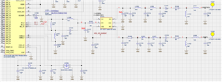
    One correction.  LAUCHXL-CC1312R results were measured before antenna matching components. Here are schematics.

    BR,

    Ari

  • Thank you for your results.

    Just to clarify about the LAUNCHXL-CC1312R work you performed - do you mean you designed a custom board based on that reference design, or something else?

    I am not sure you will get optimal output power for every band due to the insertion losses of the balun and RF switches. It may be that you need to prioritise one RF path over the other.

    Please could you provide more details on your target output power for 433 MHz? To my knowledge, 470-510 MHz allows more output power, but the 433 MHz band is limited to +10 dBm. Could you provide a link to the regulations you are aiming for if it is greater than +10 dBm?
    Regards,

    Zack

  • Hi Zack,

    First I modified TI 1312R evaluation board and after that implemented to our 1st proto and results were very promising.

    Sure I understand that if I combine 433 MHz and 868/915 MHz to same design the performance will suffer. But  with this latest design there is only about 1.5 dB power decrease in 433 MHz band compared to LAUNCHXL-CC1312R with LAUNCHXL-CC1312R output matching circuit. 868/915 MHz band power decrease should be only amount of switch loss (typical 0.18 dB).

    Actually in this base I not worried about power regulations because we can always decrease power by software, right? 

    I'm worried about bad matching which will decrease power and sensitivity and increase level of 1st harmonic. With harmonic levels that I measured for our first design we will have difficulties to meet radiated spurious emissions specification which is -36 dBm below 1 GHz.

    BR,

    Ari

  • Decreasing the output power through SW is definitely an option but we would recommend matching with the PA settings you plan to use as by changing the PA gain (via the PA settings) you will shift the optimum load of the PA.

    If the RF switch is not presented with 50 Ohms at each port there is also a risk that the RF switch will contribute to spurious emissions. The wideband balun will also introduce loss to the circuit (1 dB according to the datasheet). So at least 1.5 dB of degraded output power looks to be realistic (to be conservative).

    If you modified a CC1312R LaunchPad by adding a switch (according to the schematic sent), could you send a photo of this (just to be clear about how you did this)?

    We can move to private messaging if you would rather not share it publicly (I've sent a friend request); I will also contact your local FAE so that we can arrange a call if needed for this. 

  • Hi Zack,

    We could move private messaging. I accepted your invitation.  

    I did not implemented switch to the evaluation board. I just tested 433  MHz and 868/915 MHz separately. After that I implemented 433 MHz matching to our first proto and checked that this really works also with switches. It was actually very difficult to implement because had to remove balun and implement chip output matching circuit including wire to RX_TX pin but seems to work. When we got second proto I will do fine tuning for matching and more measurement.

    BR,

    Ari

  • Thank you, I will mark this thread as resolved and move to private messaging (otherwise this thread will flag as unanswered).