This thread has been locked.

If you have a related question, please click the "Ask a related question" button in the top right corner. The newly created question will be automatically linked to this question.

CC1311P3: General questions to evaluation kit

Part Number: CC1311P3
Other Parts Discussed in Thread: CC1311R3, ,

Dear ladies and gentlemen,

I have some questions for getting started with the evaluation kit for CC1311:

- The eval kit has differential output for rx and tx. Is there a second CC1311 board with single ended layout?

- If no separate board, is there a recommended BOM for testing single ended?

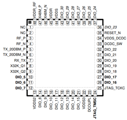
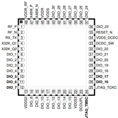
- For my eval kit there are two radio paths active, the 14dBm and 20dBm -> I think I have the P version of the chip. What happens to the high power pins for the normal not P version of the chip?

- Do you have a BOM for 10dBm optimized rf output?

- There should be any register value in SmartRF Studio for switch between single ended and differential radio front end. Which one is this?

Thank you in advance.

Best regards

Tobias

  • Hi Tobias,

    • We are developing a single-ended design for the CC1311R3/P3 - it has not been finalised or tested but will be very soon.
    • I can share the preliminary (untested) design if you want to mount the RF path on a LP-CC1311P3 for evaluation? Please let me know if this is useful or if you would rather wait.
    • You do indeed have the CC1311P3. There are two CC1311R3 variants, one 7x7 mm (RGZ) and one 5x5 mm (RKP). I have included a comparison of the pinouts between comparible P3 and R3 devices below, taken from their respective datasheets:
    CC1311P3 RGZ CC1311R3 RGZ
    CC1311P3 Datasheet: https://www.ti.com/lit/swrs255 CC1311R3 Datasheet: https://www.ti.com/lit/swrs256

    As you can see, the CC1311R3 RGZ variant has 30 GPIOs, whilst the CC1311P3 has 26 GPIOs.

    • Assuming you mean a single-ended BOM for +10 dBm output, the tradeoffs stated in Section 2.1 of SWRA640 (CC13xx/CC26xx Hardware Configuration and PCB Design Considerations): https://www.ti.com/lit/swra640 apply, so there should be an existing power setting that comes close to this. However, PA table settings will not be tested/adjusted until the design is complete (we need to evaluate the board performance first).

    The steps for configuring single-ended mode in SmartRF Studio are:

    1. Settings -> Custom Target Configuration...
    2. Under Target Selection select New
    3. Under Basic Configuration there is a Front-end drop-down menu. You can select single-ended/differential operation with either an internal/external bias.
    4.  Save your new configuration.

    Regards,

    Zack

  • Hi Zack, 

    thanks for your answer.

    What does "very soon" mean exactly? If the testing is finished, will there be also EVK´s with the single ended design?

    I would like to have a 10dBm BOM for single ended and differential ended. Are there maybe also separate EVK´s with 10dBm BOM? Soldering on 0201 components is not the easiest way for modifying that.

    Best regards

    Tobias

  • Hi Tobias,

    I have checked with my colleague who is doing the design and we won't be producing the design beyond the internal optimisation effort (but can release the reference design files on TI.com). We can probably send some of the boards to you if the timing works out, however, but I would need confirmation on how many we are producing first.

    "Very soon" is understandably a bit vague (and subjective).  The design was reviewed this week, so I can send you the preliminary design once the recommended changes have been implemented. To clarify, it will probably be several months before the board will have been optimised in the lab and tested; at least 3.

    For the 10 dBm differential BOM, you can use the +14 dBm Sub-1 GHz path of the LP-CC1311P3 design and use the +10 dBm PA table setting, assuming your design is for 868/915 MHz.

    I am a little confused about the need for a (differential) +10 dBm BOM because of the possibility to use a PA table setting for this; the performance typically is acceptable with this solution as it is not feasible to have a separate BOM optimised for every PA table setting (if I understand your reply correctly).

    I can modify 3 LP-CC1311P3 LaunchPads to use the preliminary single-ended BOM for the +14 dBm path and send them to you if you would rather avoid soldering the 0201 components and want to evaluate the boards sooner. Please let me know.

    Regards,

    Zack

  • Hey Zack,

    understood. So for the 10dBm measurements we will use the default 14dBm rf path which we already have, thanks for clarification.

    It would be great, if you could modify three boards to a single ended BOM and send them over.

    Best regards

    Tobias

  • I will modify some boards and send them - I have sent a friend request so we can discuss the logistics privately.

    Regards,

    Zack