


Other Parts Discussed in Thread: CC1190, CC1310
Hello,
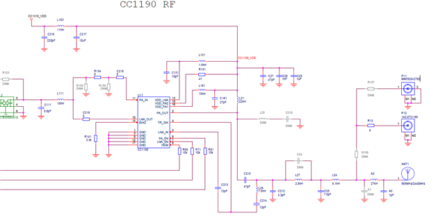
I'm working on a design involving the CC1310 and CC1190 and I'm referencing the CC1310-CC1190 Reference Design US schematics. I've referenced a few resources, including www.ti.com/.../swra542, using CC1190 with CC13xx, and www.ti.com/.../swra640g, the CC13xx hardware design guide, and had some questions about the purpose of some components. I'm adding what I think I know about some of them, please correct me if I'm wrong?
What is L24/C25 used for? I see that C212/L27 is a notch filter for harmonics, but I'm not sure why C24 is left unfilled in the current schematic? I also wanted to confirm that impedance entering the SMA connector after L24 is matched to 50 Ohms, right? I believe A2/A3 are used to match impedance for the PCB antenna included in the development board. I see that C214/L26 are used to match impedance to LNA_IN pin.
I see that C27/C28/C29 are decoupling capacitors for CC1190 supply, but what do L131/C131 and L161/C161 do? Filters against harmonics in power supply? If so why is R151 sufficient for VDD_PA2? From the pin table in the CC1190 datasheet it seems all three VDD pins serve the same purpose, so why would they have different LC values?
Thanks for any input, I appreciate it!
