This thread has been locked.

If you have a related question, please click the "Ask a related question" button in the top right corner. The newly created question will be automatically linked to this question.

CC110L: 433MHz antenna, reference design, matching network

Part Number: CC110L

Hi,

I am using your CC110L in a design of mine. I am targeting 433MHz. A few questions on the implementation:

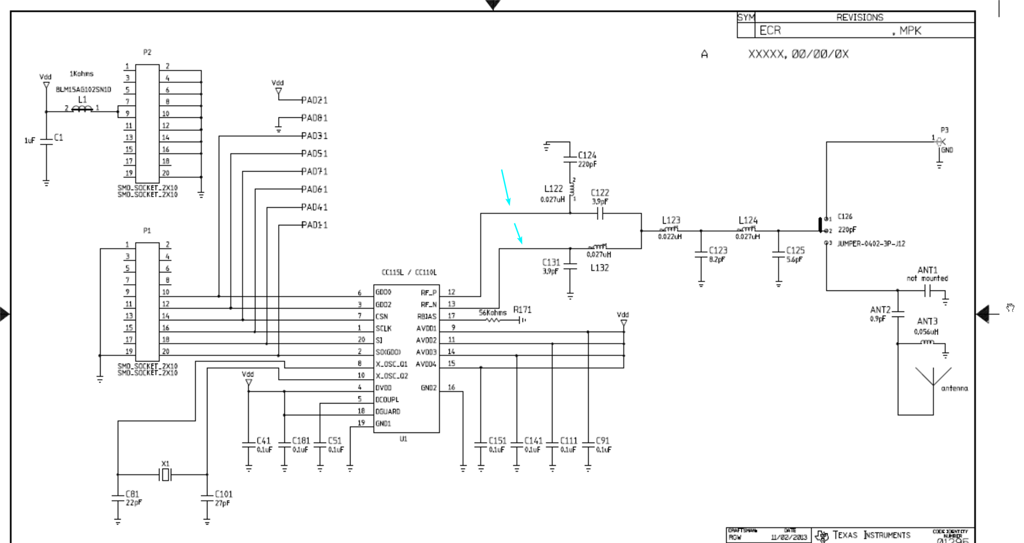
1) If I use the helical PCB antenna you used in reference design SWRR081, can I copy the balun and matching component values exactly and expect a perfectly matched antenna? Do I need to tune those values? I think I will always need to retune the matching components due to my PCB shape, case size, and amount of ground plane being different (even if I use the same stack up and board material). Below is the schematic for reference:
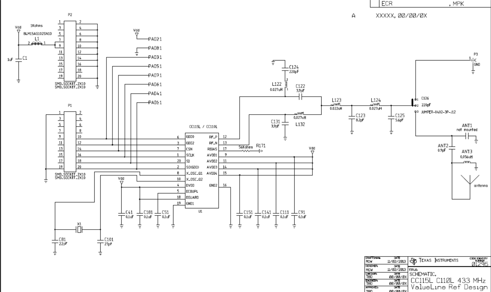
2) Do I need to retune the balun values used in reference design SWRR081? Or will those always be correct?

3) How do you figure out what the antenna-matching component values should be? If this was an unbalanced/single ended application, then you could connect a VNA to the transmit signal pad of the IC, measure it, and tune it as necessary. This is a balanced/differential output so I don't think I can use a standard VNA here. Is that correct? Do you have a good application note for taking this measurement?

4) In Application Note AN058, you recommend using Pulse antenna W3127. Is there a reference design for this antenna that uses CC110L part? I'm unsure of what the antenna-matching component values should be. Will the balun values change?

Thanks,

Brandon

  • Hi Brandon,

    1. The balun and filter components can be copied directly to the DC blocking capacitor C126. This design was based on 0402 passives which was the most standard passive size of the components when this was released. Using the same size of passives, then these component values can just be re-used.

    2. Re-use values but keep with 0402.

    3. We always terminate our designs to a 50 ohm load. i.e. after C126 should be close to 50 ohm. From this point the antenna design is also matched to 50 ohm load. In order to tune the antenna, C126 should be removed which disconnects the radio section completely. Refer to section 6.2 in the app note https://www.ti.com/lit/swra161 for more info on measuring the antenna. When you have measured the natural impedance of your antenna on a VNA, then the antenna match can be determined. The antenna match will be dependent on the size of your GND plane, antenna placement, physical casing of DUT and place of DUT near other object, so ANT1, ANT2 & ANT3 will always be unique for each final product.

    4. Just copy the antenna ref design for W3127 since this will be to a 50 ohm interface. 

    Let me know if you have any problems matching the antenna or performance issues. What's important with compact 433 MHz designs is to calculate on a realistic antenna efficiency due to the physical size. At 868/915/2440 MHz, a high efficiency can be achieved for hand-held devices. This is not the case when operating < 433 MHz due to the wavelength. This is regardless of the antenna topology. 

    Regards,

       Richard

  • Hi Richard,

    Thanks for all this great info! Really great guidance!

    I will copy all values up to C126 as you suggested. I am using all 0402 parts on this design, so that works out nicely.

    I will leave placeholders for ANT1 (leave as open), ANT2 (0 ohm res), and ANT3 (leave as open) as it sounds like those are the components I will use to tune the antenna to 50 ohms using a VNA.

    Another question: Will pulse antenna W3127 be more efficient than the PCB helical antenna used in the reference design above? I'm not sure if the additional 1 dollar for the pulse antenna is worth it or maybe I stick with the free PCB helical antenna. 1 dollar isn't a significant BOM cost for my design, but just trying to get a better understanding of the tradeoffs between the 2 options.

    Thanks,

    Brandon

  • Hi,

    Can you send a layout picture of your board showing the antenna and the GND plane ?

    The only time I would recommend a chip/wire antenna is when the x,y & z dimensions are utilized more than just the x and y dimensions. i.e. greater utilization of the available volume instead of just PCB area.  One main advantage with chip/wire antennas, is that the chip/wire antenna vendor can assist in matching your antenna on your board. 

    I would expect a greater efficiency with a wire helical antenna than the PCB helical antenna due to greater utilization of volume. Also, the wire helical antenna will not be sensitive for variations in PCB thickness.

  • Hi Richard,

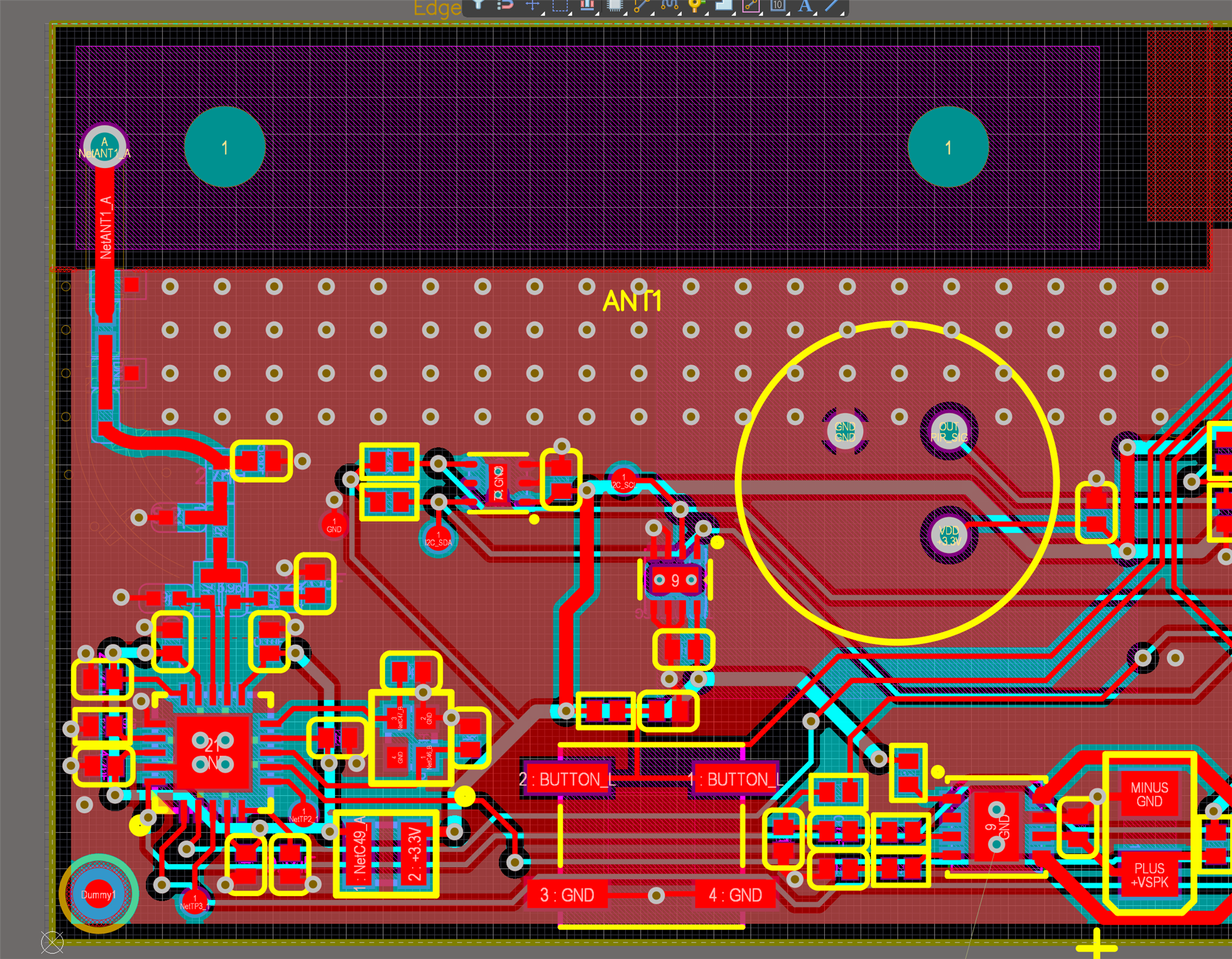
    Below is a snapshot of my current layout. I decided to go with the wire antenna since it should have better efficiency and the documentation from pulse was very good. I still need to add ground stitching vias along the CPW trace going out to the antenna as well as general ground stitching vias across the board.

    Another item I need some help with: what should the impedance of the RF_P and RF_N traces be? 50 ohms single ended? I copied the balun component values and placed them exactly as was done in the reference design. My stackup does not line up with what they used though, so I have to be careful about copying their trace widths. The reference design had FR4 with a distance of 31.5mils to the ground plane, mine is also FR4 but a 4-layer stack up so the distance to the ground plane is significantly less (can be anywhere from 5-20 mils as needed for trace widths/impedances).

    Thanks for your help!

    Brandon

  • Hi Richard,

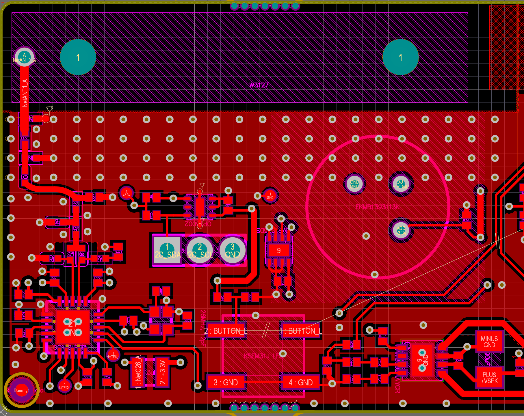
    I'm about wrapped up with the layout of the board and wanted to share with you an updated layout of the RF section. It is below. Other than figuring out the trace widths (see question above) this should be final. Please let me know how to handle the trace widths in the RF Balanced trace section.

    Brandon

  • Hi, 

    The passive balun network should be placed closer to the chip as in the original design. This is more important than the placement of the bypass caps. 

    Is there GND to the right of the antenna (top, right) ? If possible, I would remove this GND area in the top right corner next to the antenna.

    If the antenna is placed at a greater distance from the GND plane, then the antenna efficiency will be improved. Unfortunately, this will be a size 'v' efficiency compromise. If the antenna is rotated 90 degrees to the left; then this will give a greater efficiency and bandwidth. But this will increase the overall size.

  • Hi Richard,

    thanks for your input!

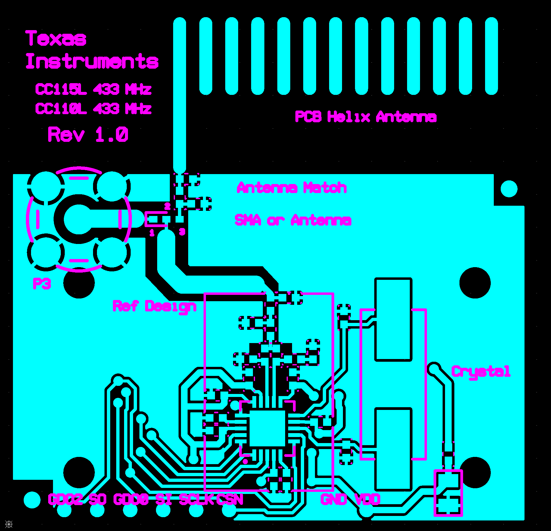
    For the balun network, I copied the exact placement as was used in reference design SWRR081. It is below for your reference. You'll see that the decoupling caps are closer to the part than the balun network (but I agree with you that the balun network should be close to the chip). I believe I should maintain the same distance as was used in the ref design, otherwise the balun values will probably not be correct. Please let me know if my understanding is incorrect.

    For distance to the ground plane, I copied the same distance as was used in the pulse reference design. I will remove more of the ground in the top right--good suggestion!

    Due to board shape, i cannot rotate it 90 degrees. Can you explain what you mean by "size 'v' efficiency compromise"? I'm not familiar with that term.

    Thanks!

    Brandon

  • Hi Brandon,

    You are correct here regarding the placement of the placement of the balun components so ignore previous feedback :) Good that you have copied the reference design of CC11xL.

    Size 'v' efficiency: the quarter wavelength for 433 MHz is 17.3 cm which is much larger than this design. Therefore, the antenna is small and ideally should be much larger. If we look at the effective size of the antenna and the GND plane we will have a certain area size. If we increase this area size by extending the GND plane of by rotating the antenna 90 degrees; we will make the effective area size larger.

    A larger effective antenna area size will give a greater antenna efficiency and increase the bandwidth. Also, if the antenna was rotated 90 degrees to the left, there would be less loading to the GND.