

Other Parts Discussed in Thread: CC1352R,
Hi,
In the application note (swra629a), layout of traces between CC1352R and balun is done in the following way, with straight and symmetric traces of RF_N/P.
But for CC1352P, since we need to make room for 20dBm RF signals, it becomes difficult to copy the layout of CC1352R. We have two options:
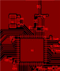
Option 1: straight and symmetric traces between CC1352P and balun for low-power RF signals, long and sort of symmetrical traces for 20dBm RF signals, something like the following:
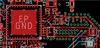
Option 2: bent and mostly symmetric traces for low-power RF signals, but shorter traces for 20dBm signals, something like the following:
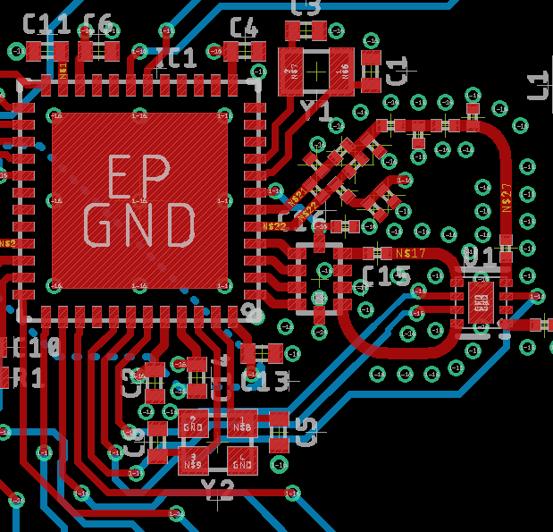
application note (swra629a) has very strict recommendations on the layout of those traces, including trace width, distance between balun and CC1352.
My questions are:
1) Does option 2 still meet the recommendation of SWRA629A?
2) Will the 20dBm RF signals in option 1 work OK?
Please advise.
Thanks,
ZL
