This thread has been locked.

If you have a related question, please click the "Ask a related question" button in the top right corner. The newly created question will be automatically linked to this question.

LAUNCHXL-CC1312R1: balun

Part Number: LAUNCHXL-CC1312R1
Other Parts Discussed in Thread: CC1312R

Thank you for answering

[question 1]
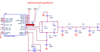
We found that the optimal load impedance for the circuit below is:
optimun Load Impedance (40 + j15 Ω) @ 868MHz on swra640g.pdf page 29


So, what is the optimum load impedance for 315MHz, 430MHz, 920MHz, and 1200MHz?

[Question 2]
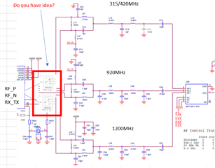
I understand that designing a broadband balun is difficult.
For example, is it possible to consider using a switch as shown below?
If you have any ICs made by TI that could be used, please let me know.

best regards

  • Hi,

    A triple-band design with one CC1312R device is quite ambitious.

    1.

    We strongly recommend that customers directly copy our reference designs for each of those frequency bands. Additionally:

    • We typically recommend the same match for 315/433 MHz and also (separately) 868/915 MHz as the designs have good performance across those bands.
    • We do not currently have a reference design for 1200 MHz, so this may require additional work.

    2.

    We do not recommend placing an RF switch at the device pins for several reasons:

    • The switch, by design, provides isolation between the input/output ports and therefore actually makes impedance matching more difficult.
    • RF switches are typically designed for a 50 Ohm input/output impedance. Whilst they usually have some tolerance to impedance mismatch, the more mismatch there is, the more non-linear behaviour RF switch could display. This will result in spurious emissions and other unwanted behaviour.
    • As the PA/LNA require specific impedances to be presented at each band in order to produce the desired performance, you would by design have to intentionally mismatch the RF switches. In addition to the spurious emissions mentioned above, the match(es) would be sub-optimal. Therefore, we recommend trying to perform the impedance matching for the RF front-end before any RF switches where possible.
    • You would need a single switch for the RF_P/RF_N paths rather than two switches (i.e. don't use one switch on each pin).
    • You would likely need to reoptimise each RF matching network/filter with this approach.

    If a lower output power (~+10 dBm) is acceptable, you could consider single-ended networks for a dual-band design (315/433 MHz and 868/915 MHz) which would then remove the need for the baluns. This comes with drawbacks to RX Sensitivity and TX Output Power - please see SWRA640 for more information. Note that using several RF switches would mean that the insertion losses of the switches would need to be considered, meaning the trade-off of may make sense.

    Alternatively, a wideband balun and then developing a match that gives the best performance at 868/915 MHz, with reduced performance at 315/433 MHz and/or 1200 MHz is the other option. It is unlikely to be possible to achieve optimal performance at all desired bands with only one CC1312R device.

    Regards,

    Zack