Other Parts Discussed in Thread: LP-XDS110ET, , CC1312R
Tool/software:
Hello
Please be so kind to refer to the description and question below:
Setup:
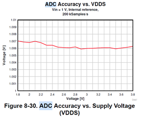
A proprietary board with CC1312PSIP. The code utilizes Sensor Controller ADC to sample an analog input.
The ADC's reference is VVDS and it is operated in synchronous fashion with scaling turned on and a manual trigger.
We also use AUXADCAdjustValueForGainAndOffset() on the retrieved ADC result to increase the result's accuracy
The issue at hand:
We keep seeing deviations in ADC value with the ADC's result being ~20mV to ~50mV lower than expected.
The deviations seem to increase as a function of the input voltage's magnitude (with 3.3V being the maximum).
E.g. in the current test setup and in conditions where we expect to get 3.3V (0xFFF) - we get 3.287V (0xFEE)...
Questions:
1) Should there be a settling time from the moment the ADC is enabled, triggered and read?
1.1) If yes - what is the recommended delay and how should it be distributed between enabling, triggering and reading?
2) The ADC can receive either a relative reference voltage (VDDS) or a fixed reference. When using a relative reference - how does the ADC retrieve the voltage?
2.1) Is the ADC reference inlet simply being routed to connect to VDDS thereby receiving an analog value or
Is the reference a value kept is a register that is being read by the ADC while VDDS sampling is performed by other mechanism in the chip.
2.2) If the latter in (2.1 is the correct operation description - is VDDS sampled voltage kept in register BAT @ AON_BATMON Registers, offset 0x28?
2.2.1) What is the reference used to sample VDDS in BAT register?
2.2.2) Does the returned value of function AONBatMonBatteryVoltageGet() give accurate representation of the VDDS value used by the Sensor Controller's ADC?
Thank you so much
/Gil