This thread has been locked.

If you have a related question, please click the "Ask a related question" button in the top right corner. The newly created question will be automatically linked to this question.

CC1352R: Dual sub-giga RF chain

Part Number: CC1352R
Other Parts Discussed in Thread: CC1352P, CC1350

Tool/software:

Hello,
I want to use CC1352 with both 915 & 433Mhz frequency. (Not at the same time - but support these 2 configurations)
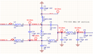
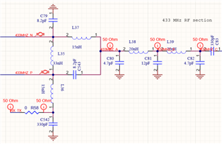
I know that CC1352 can tune the sub-giga frequency, but there is a different recommended filter chain for every frequency.
My question is what is the recommended design for that use case? Or should I use a different IC that supports 2 sub-giga outputs?

Thanks in advanced 

  • Hi,

    Recommend to use two single-ended configurations with the CC1352R; one for the 915 MHz and the other for the 433 MHz.

  • OK. Can you please share your recommended chain design for each frequency in single-ended mode?

    This is the designs I know for the differential use:
    915Mhz:

    433Mhz:

  • Hi,

    I will reply on Monday regarding the recommended topologies; is the CC1352P an option? What is your timeframe? This helps decide on what recommendation to give.

    Regards,

    Zack

  • Hi,
    If the CC1352P is FW compatible (registers etc') to CC1352R then it's an option.

    Waiting for your answer, Thanks!

  • Hi, do you have a recommendation? 

  • Hi Ofer,

    Sorry for the delay, I am clarifying the 915 MHz single-ended topology internally and then I can provide the schematics and BOM.


    A further question: will you be using a 0402 or 0201 SMD component size for the RF path?

    Regards,

    Zack

  • Thanks Zack,
    0402 only

  • Hi Ofer,

    Our most up-to-date preliminary designs have been developed for a 0201 component size (see Section 2.4 of SWRA814 (SimpleLink CC131x and CC135x Family Hardware Migration Guide) https://www.ti.com/lit/swra814 for reasons this could result in performance differences).

    The most time-efficient approach I would take is to use the preliminary designs below as a starting point. Although the 433 MHz BOM is stated as being for the CC1350, this should still be valid.

    The 433 MHz BOM (ignore the 2.4 GHz path):

    For 868/915 MHz, the BOM provided in Section 2.3.1 of SWRA640 (CC13xx/CC26xx Hardware Configuration and PCB Design Considerations): https://www.ti.com/lit/swra640:

    To minimise risk, for the 868/915 MHz BOM I would add an additional series inductor after C2 (before the shunt capacitor C3) and mark it as 0R for now, just so you have more flexibility with the design. This means the basic topology is the same for both 433 MHz and 868/915 MHz (which also simplifies the layout). 

    This hasn't been forgotten about, but we cannot assign a large amount of resources to optimising a new BOM if it is not a large order size so I am seeing what can be done. As it is the Easter break here (national holiday), I will need to continue following this up next week.

    Regards,

    Zack