This thread has been locked.

If you have a related question, please click the "Ask a related question" button in the top right corner. The newly created question will be automatically linked to this question.

CC1312R7: Demodulated data output strange shape

Part Number: CC1312R7
Other Parts Discussed in Thread: CC1310, CC1312R

Tool/software:

Hi

In my system I have basicaly two type of device: network manager (NM) and end unit (EU). GFSK modulation, 50kBits/s, RF band 868MHz.

The NM run on a TI CC1312R1 LaunchPad. EU run on a CC1312R7 LaunchPad or on a real (custom) HW with CC1312R7.

The communication between devices looks like to work OK (frames are received, CRC pass, decryption pass, and ACKs are send back).

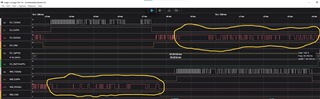
The Issue is that the demodulated RX data output by RF cores of both NM and EU looks very strange in case that EU runs on a custom HW. 

Any ideas what could be wrong?

Screenshot from a logic analyzer to show you the signals: 

Regards,

Dimitar

  • Hi Dimitar,

    could you explain me in more detail which is the issue that you are seeing?
    Is something failing in your application?
    And what would you expect instead?

    Thank you in advance,
    Theo

  • Hi Theo,

    are you familiar with this: Routing RF Core Signals to Physical Pins, if not please became.

    I have an application that looks like to work. The issue is that this signal:

    MCE_GPO1†   Binary data signal that comes from the demodulator when receiving.

    that cames from RF core not looks like as a RF frames and I expectthey to looks like as such especially if from the application point ow view communication pass (the image shows frame sent from EU and acknowleged by NM). 

    So my question Is why the demodulated data of received frames that the RF cores output (surround  with yellow line) look so strange, when the frames are received as good? 

    Regards,

    Dimitar   

  • Hi Dimitar,

    thank you for the details.

    The issue here is that routing the rf core signals to physical pins is meant for debug purposes only.
    The rf core is performing additional processing of the received data meaning that even if the data does not look good on the pin the rf core is able to interpret the data correctly. This is why your application is showing no errors.

    When you use the debug signal to interpret the packet from the pin you will not get the same sensitivity as when letting the rf core handle the data.

    Kind regards,
    Theo

  • Hi Theo,

    I am definately not going to use the signal from the pin to interpret the packet.

    As I already wrote if I run the program on a launchpad the signal looks like quite good, but it is bad if it run on a custom board. In both cases the boards (EU) are on the same distance to the NM device and the RSSI is big enought (not less than -30dBm). There is around 17kHz frequency offset between NM and EU devices in case of EU run on a custom boart, so do a test with RX BW set to 155kHz (98kHz originaly), but I still don't see a goot RX data shape.   

    So my question was and still is: What can cause the difference in the RX deta signal signal?

    I think that someone of your RF HW team could give me the right answer or at least point me in the right dirrection.

    Regards,

    Dimitar       

  • Hi Dimitar,

    Is the GPIO configuration of the GPIO being used for the MCE_GPO1 signal the same when running on a LP and the custom HW? I assume they are running the same firmware, therefore same GPIO configuration, but I would like to confirm this.

    In the original post, you mention that the data rate is 50 kbps, but I see no mention of the deviation. Is it 25 kHz or another value?

    Have you compared the frequency offset between the LP and the custom HW? The signal from MCE_GPO1 can change depending on frequency offset because is output to the pin before any frequency error compensation.

  • Hi Diego,

    I have preset "This resolve my issue" button by mistake. 

    "Is the GPIO configuration of the GPIO being used for the MCE_GPO1 signal the same when running on a LP and the custom HW? I assume they are running the same firmware, therefore same GPIO configuration, but I would like to confirm this." - Yes, the same softwee and GPIO configuration. 

    In the original post, you mention that the data rate is 50 kbps, but I see no mention of the deviation. Is it 25 kHz or another value? - Yes, 25kHz, the settings are from the RF smart studio v.7.2.28. The band is 868MHz and the TX power in this test was +3dBm (going to be 12.5dBm finally).  

    Have you compared the frequency offset between the LP and the custom HW? The signal from MCE_GPO1 can change depending on frequency offset because is output to the pin before any frequency error compensation. - Frequency offset of two boards compared to the NM board: LP has -4kHz, custom board has 17kHz.   

    I am not going to use this signal to decode packets. I rise this conversation to understod if there could be something wrong with the custom HW that going to stay hidden.

    Let me ask two more questions:

    1. Knowing what are capabilities of CC1312R7 receiving part does you/TI thing that implementing of frequency offset compensation in the devices is still good idea (I have used such in some of my old projects based on CC1110)?

    2. The RX BW for the setting that I am using (came from smart RF studio) is 98kHz. The question is the XOSC whit how many ppm accuracy cover this value?

    Regards

    Dimitar   

  • Hi Dimitar,

    In the CC1310 datasheet there is a PER vs input RF level vs frequency offset plot for 50 kbps 25kHz deviation PHY. Although this is not in the CC1312R7 datasheet, you should see similar offset tolerance performance on the CC1312R7.

    It should handle about a 35 ppm offset, greater than this you would see significant sensitivity degradation until packets are not received at all at about 45 ppm offset.

    Are you using the same crystal as the crystal on the CC1312R7 reference design? The reference design uses the cap array to load the crystal. If you use a crystal with a different load capacitance and maintain the default cap array value, then the frequency offset can be greater with you crystal than the reference design crystal.

    Or are you using external load caps and turning off the cap array?

  • Hi Diego,

    I am aware abour cap array existance, and that it shoud be tuned acording to the crystal and PCB, but I am not the HW developer. 

    There are no external load caps for sure. The cap array is on its default (should be 6.7pF for CC1312R according mentation). By the way, does capacistance of caps array is given as total load capacitance on both pins (the needed load capacitance according to the crystal datasheet) or only on one of the pins?

    According to HW developer we use this cristal:

    NX2016SA-48M-EXS00A-CS05517-Spec-Sheet.pdf

    Regards,

    Dimitar 

  • Hi Dimitar,

    Yes, capacitance of the cap array is the total load capacitance for the crystal. A full table of the capacitance vs. cap array delta can be found in section 6.4 of CC13xx/CC26xx Hardware Configuration and PCB Design Considerations