This thread has been locked.

If you have a related question, please click the "Ask a related question" button in the top right corner. The newly created question will be automatically linked to this question.

CC1190 with CC110L no Amplification

Other Parts Discussed in Thread: CC110L, CC1190, CC1101

HI,

We are working on a design that uses the CC110L together with the CC1190 range extender chip as a transmitter unit and a single CC110L as a receiver. The communication works for short distances (within one room). However, the output power at the antenna is very low.


Our design is directly derived from the reference design (cc1101 with cc1190). Schematic and Layout are appended:

5670.cc110l_baseboard_sch.pdf

2870.cc110l_baseboard_brd.pdf


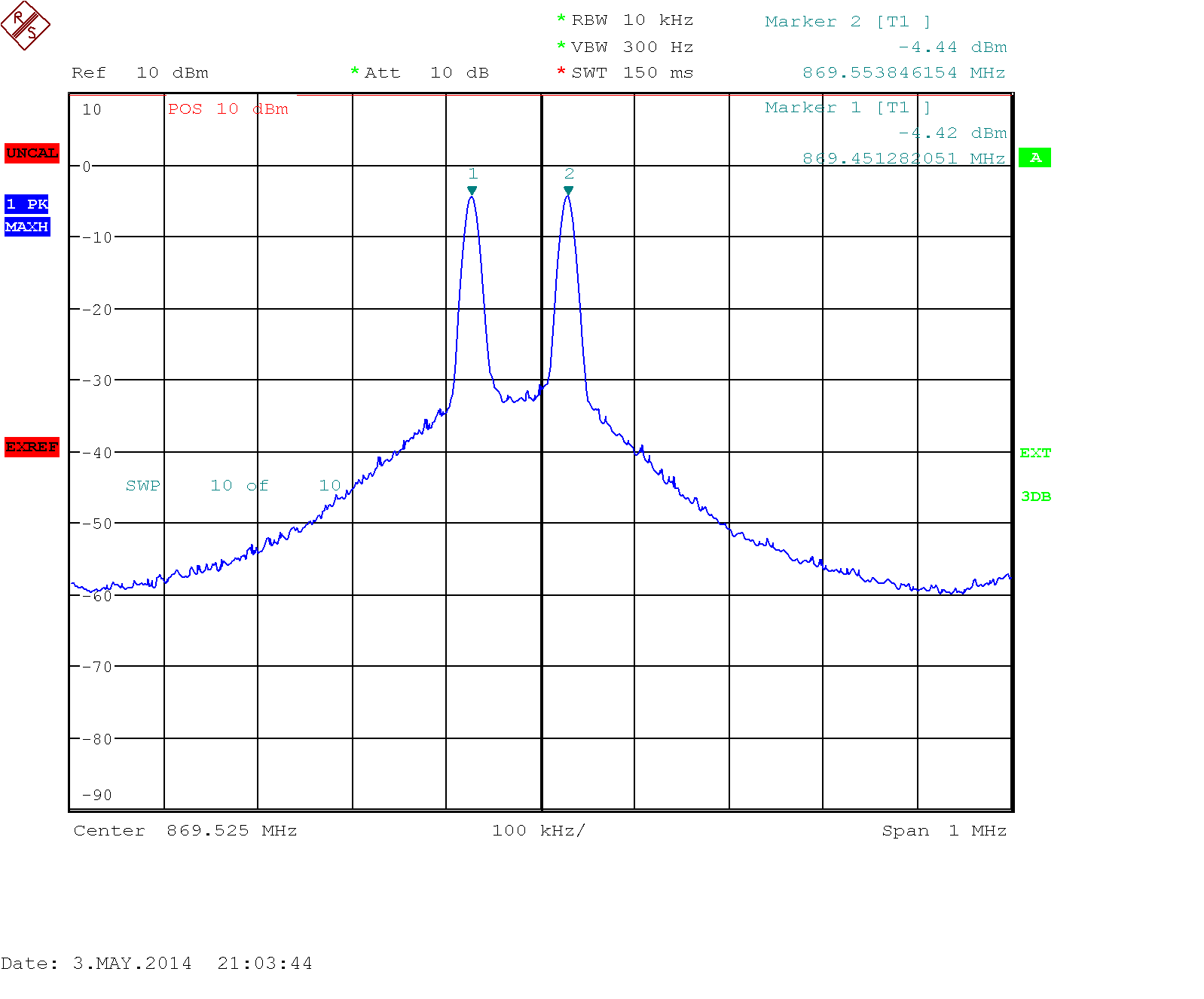
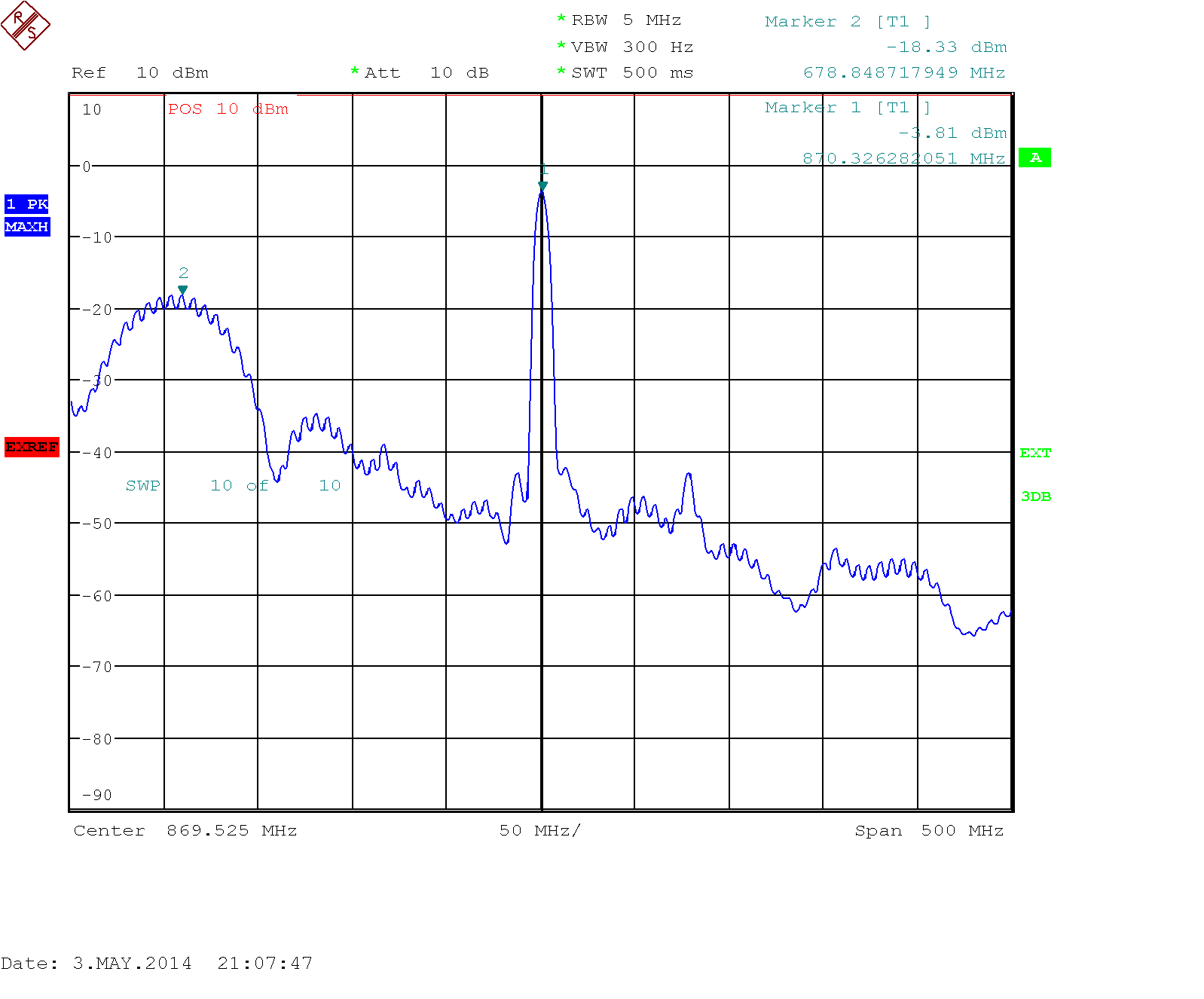
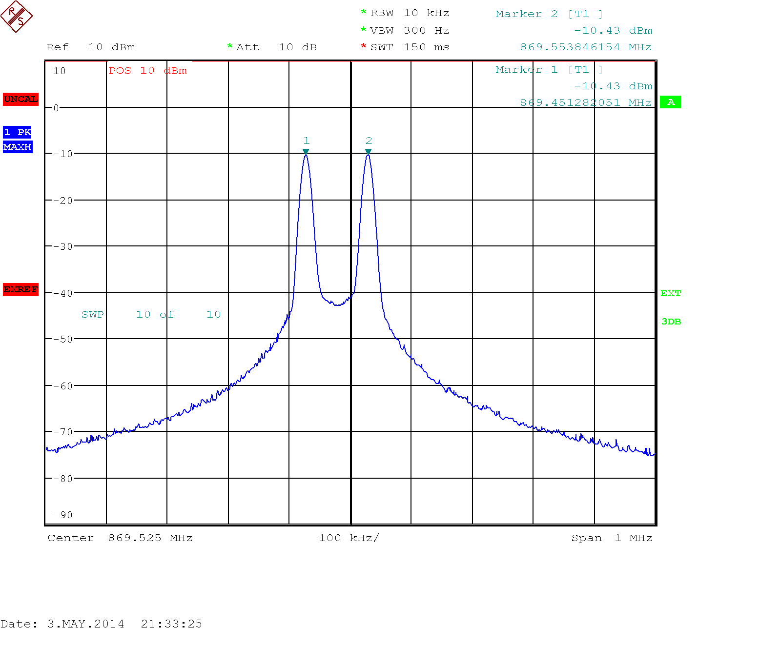
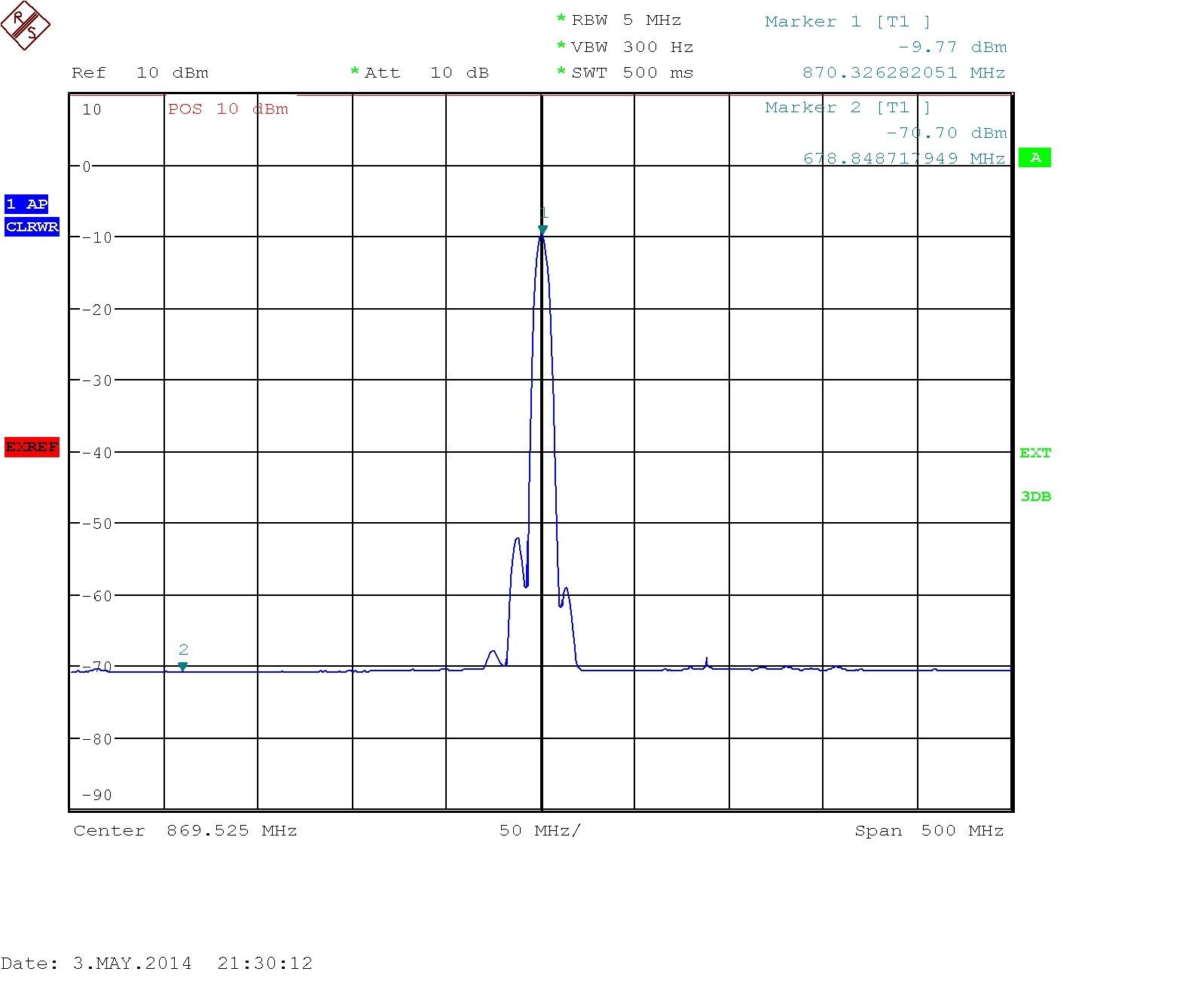
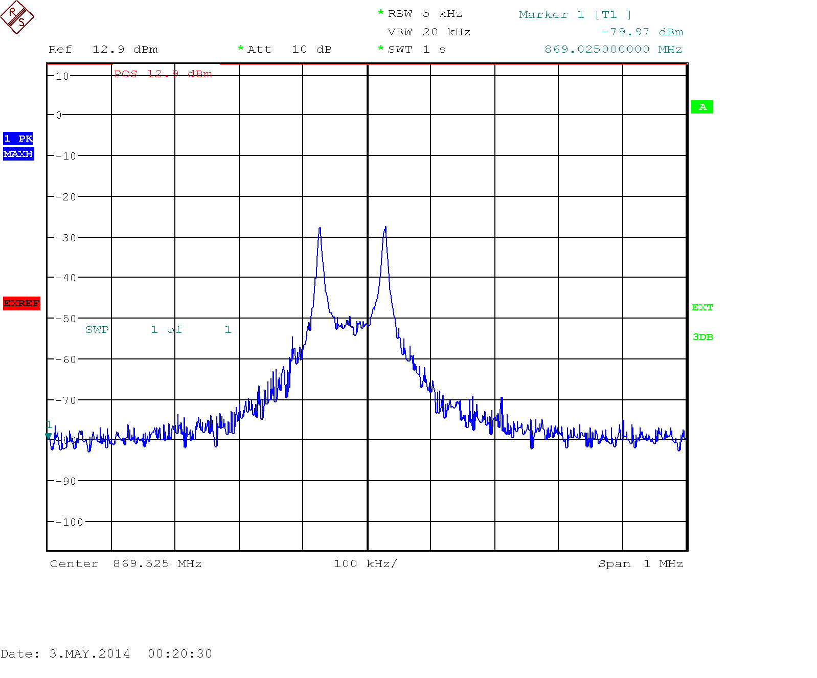
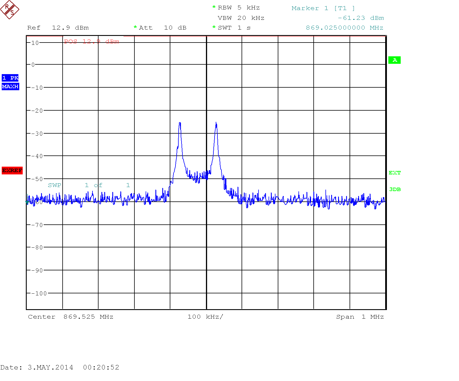
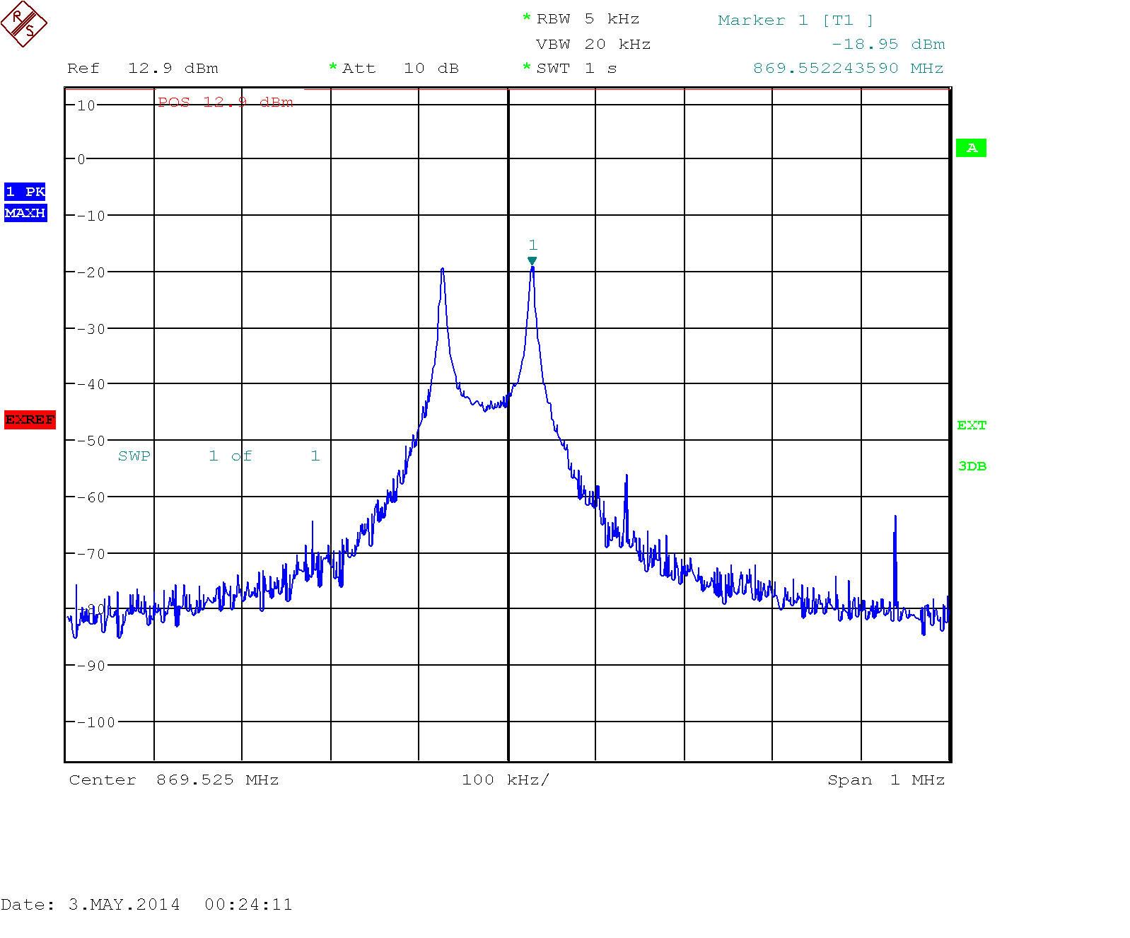
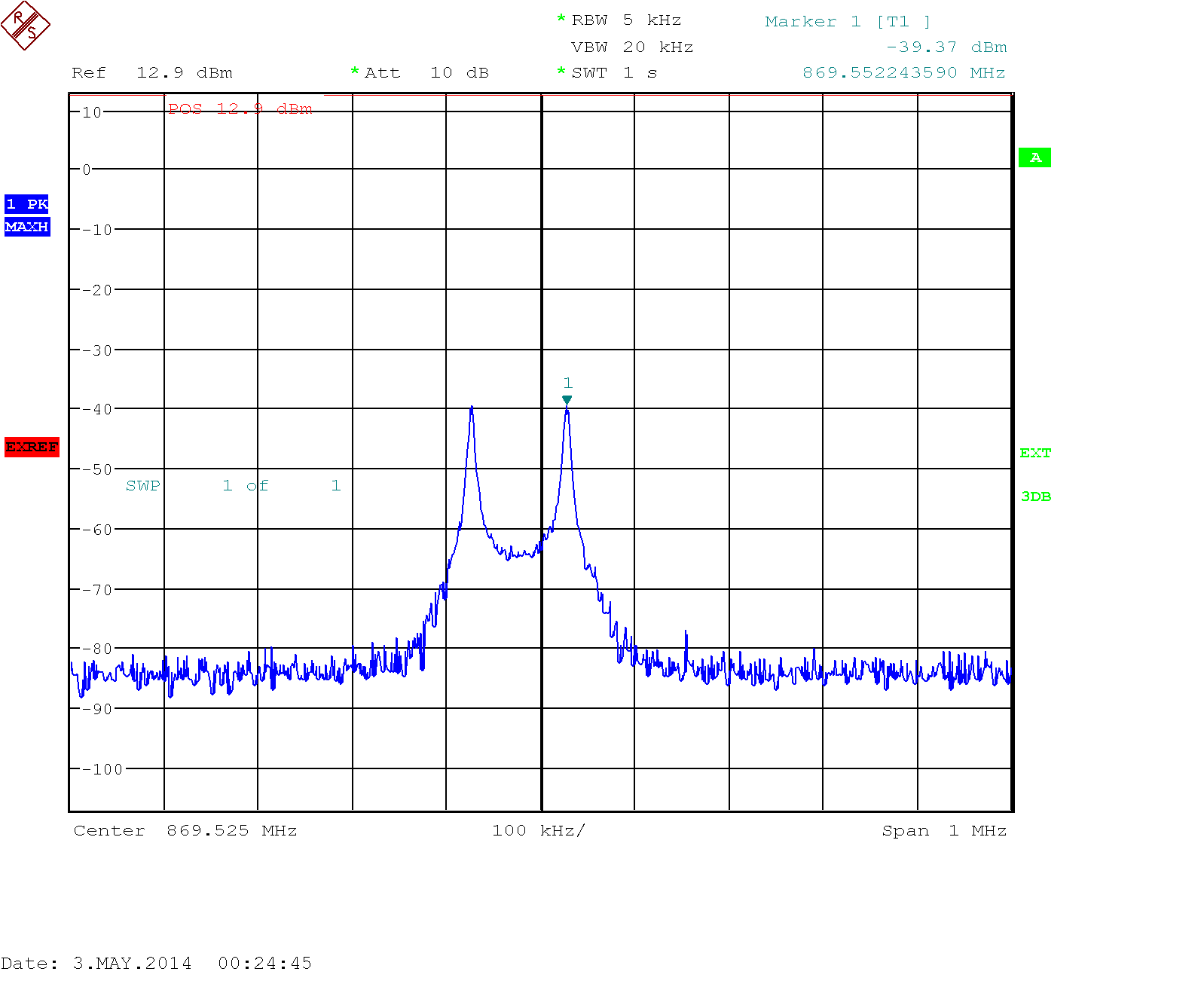
A look at the spectrum analyzer revealed that the noise seems to be amplified but not the signal itself. These values were conducted by using a test probe to pick up the values directly from the pcb. Therfore the exact amplitudes in the plots might not be accurate.

Signal in front of the CC1190 (CC1190 enabled):

Signal behind of the CC1190 (CC1190 enabled):

Signal in front of the CC1190 (CC1190 disabled):

Signal behind the CC1190 (CC1190 disabled):

These are the used register settings:

static const registerSetting_t cc110LSettings[] = {
		{CC110L_ADDR			,0x00},	/* ADDR          Device Address                                 */
		{CC110L_CHANNR			,0x00},	/* CHANNR        Frequency channel default 0x00                 */
		{CC110L_FSCTRL1			,0x06},	/* FSCTRL1       Frequency Synthesizer Control                  */
		{CC110L_FSCTRL0			,0x00},	/* FSCTRL0       Frequency Synthesizer Control                  */
		{CC110L_MDMCFG4			,0x85},	/*(F4) MDMCFG4       Modem Configuration                        */
		{CC110L_MDMCFG3			,0x83},	/*(83) MDMCFG3       Modem Configuration                        */
		{CC110L_MDMCFG2			,0x0B},	/* MDMCFG2       Modem Configuration                            */
		{CC110L_MDMCFG1			,0x20},	/* MDMCFG1       Modem Configuration                            */
		{CC110L_MDMCFG0			,0x12},	/* MDMCFG0       Modem Configuration                            */
		{CC110L_DEVIATN			,0x50},	/* DEVIATN       Modem Deviation Setting                        */
		{CC110L_MCSM2			,0x07},	/* MCSM2         Main Radio Control State Machine Configuration */
		{CC110L_FOCCFG			,0x16},	/* FOCCFG        Frequency Offset Compensation Configuration    */
		{CC110L_BSCFG			,0x6C},	/* BSCFG         Bit Synchronization Configuration              */
		{CC110L_AGCCTRL2		,0x03},	/* AGCCTRL2      AGC Control                                    */
		{CC110L_AGCCTRL1		,0x40},	/* AGCCTRL1      AGC Control                                    */
		{CC110L_AGCCTRL0		,0x91},	/* AGCCTRL0      AGC Control                                    */
		{CC110L_RESERVED_0X20	,0xFB},	/*RESERVED_0X20    Reserved register                      */
		{CC110L_FREND1			,0x56},	/* FREND1        Front End RX Configuration                     */
		{CC110L_FREND0			,0x10},	/* FREND0        Front End TX Configuration                     */
		{CC110L_TEST2			,0x81},	/* TEST2         Various Test Settings                          */
		{CC110L_TEST1			,0x35},	/* TEST1         Various Test Settings                          */
		{CC110L_TEST0			,0x09}	/* TEST0         Various Test Settings                          */
		{CC110L_IOCFG2			,0x29},	/* IOCFG2          GDO2 Output Pin Configuration (CHIP_RDYn)         */
		{CC110L_IOCFG1			,0x2E},	/* IOCFG1          GDO1 Output Pin Configuration (high impedance)    */
		{CC110L_IOCFG0			,0x06},	/* IOCFG0          GDO0 Output Pin Configuration
		(Asserts when sync word has been sent / received, and de-asserts at the end of the packet. In RX, the
		pin will also de-assert when a packet is discarded due to address or maximum length filtering or when
		the radio enters RXFIFO_OVERFLOW state. In TX the pin will de-assert if the TX FIFO underflows.     */
		{CC110L_FIFOTHR			,0x47},	/* FIFOTHR         RX FIFO and TX FIFO Thresholds                    */
		{CC110L_SYNC1			,0xD3},	/* SYNC1           Sync Word, High Byte                              */
		{CC110L_SYNC0			,0x91},	/* SYNC0           Sync Word, Low Byte                               */
		{CC110L_PKTLEN			,0xFF},	/* PKTLEN          Packet Length                                     */
		{CC110L_PKTCTRL1		,0x04},	/* PKTCTRL0        Packet Automation Control                         */
		{CC110L_PKTCTRL0		,0x05},	/* FREQ2           Frequency Control Word, High Byte                 */
		{CC110L_FREQ2			,0x21},	/* FREQ1           Frequency Control Word, Middle Byte               */
		{CC110L_FREQ1			,0x71},	/* FREQ1           Frequency Control Word, Middle Byte               */
		{CC110L_FREQ0			,0x7A},	/* FREQ0           Frequency Control Word, Low Byte                  */
		{CC110L_MCSM1			,0x30},	/* MCSM1           Main Radio Control State Machine Configuration    */
		{CC110L_MCSM0			,0x18},	/* MCSM0           Main Radio Control State Machine Configuration    */
		{CC110L_FSCAL3			,0xE9},	/* FSCAL3          Frequency Synthesizer Calibration                 */
		{CC110L_FSCAL2			,0x2A},	/* FSCAL2          Frequency Synthesizer Calibration                 */
		{CC110L_FSCAL1			,0x00},	/* FSCAL1          Frequency Synthesizer Calibration                 */
		{CC110L_FSCAL0			,0x1F},	/* FSCAL0          Frequency Synthesizer Calibration                 */
		{CC110L_RESERVED_0X29	,0x89},	/* RESERVED_0X29   Reserved register                                 */
		{CC110L_RESERVED_0X2A	,0x7F},	/* RESERVED_0X2A   Reserved register                                 */
		{CC110L_RESERVED_0X2B	,0x63},	/* RESERVED_0X2B   Reserved register                                 */
};


Do you have any idea why the amplifier might not work in our design?


Greetings,

Emil Kallias

  • 1. Can you remove the SAW filter from the board and measure the conducted output power with a 50 ohm semi-rigid cable instead of a probe so the exact conducted output power from CC110L can be measured at C123 ?

    Measure the output power with a static tx carrier.

    2. Remove CC1190 and assemble SAW filter. Measure the conducted output power after the SAW filter.

    Need to confirm the conducted power entering CC1190.

    Regards, Richard

  • Thank you, Richard, for the quick response!


    Appended you find the requested plots. I made all measurements with the output power set to PA_TABLE0 = 0x54. I also used the CC110L to transmit a continous random signal (PKTCTRL0 = 0x22; MDMCFG2 = 0x08; IOCFG0 = 0x0C).

    Static Signal 1MHz span, measured behind C123 with removed SAW:

    Static Signal 500MHz span, measured behind C123 with removed SAW:

    Static Signal 1MHz span, reassembled SAW, removed CC1190:

    Static Signal 500MHz span, reassembled SAW, removed CC1190:

    Regards, Emil Kallias

  • Hi,

    Your output power levels from the CC110L are low. I would expect around 0 dBm and you are measuring around -4 dBm and after the SAW filter I would expect around -2.5 dBm and you are measuring -10 dBm.

    The layout does not look good and I presume that this is the root cause. It appears that your design is a 2-layer board with very little grounding especially around the RF sections. 

    Regards,   Richard

  • Hi,

    Sorry I accidentally send you a version without the filled polygons. Please find appended the actual design. However I still agree that our design is not ideal. Thanks for pointing that out. It will be addressed in future versions.

    8372.cc110l_baseboard_brd_gnd.pdf

    However, to me that does not explain, that the cc1190 is not amplifying the signal at all. According to the datasheed P_out of the cc1190 should still be above 10dBm with P_in being -10dBm.

    Greetings, Emil

  • I find it a bit strange that you don't get any amplification but on the other hand your layout is poor. CC1190 is dependent on a solid ground plane. It could also look like you are using 0603 components that increase the parasitics and due to the increased size the layout will not be very optimum. I also find it a bit hard to follow the signal path out from CC1190 which should not be the case.

  • I always like to verify the obvious. Did you check the control signals from the Mega328 to the CC1190 to make sure they are in the proper state for RX or TX mode?

  • First of all, thank you very much for the response! I checked the control-signals of the CC1190 and they worked perfectly. Nevertheless we could not manage to make the design work.


    We decided to develop a new board that is much closer to the reference designs of TI (CC1101-CC1190EM 869 MHz Reference Design) and the Johanson Technology Balun Filter (used as described in Design Note DN025). However our goal was to stick to a two layers design and minimize the PCB size.


    If it is not to much to ask I would really appreciate your input on this new design before we order the PCB prototypes.

    7002.cc110l_baseboard.pdf

  • From the attached it's difficult to see the ground layer properly. Please add a file showing the two layers separately.

  • I was not able to upload Gerber Files, but i hope these pdf's will do.

    7737.cc110l_baseboard_top_layer.pdf

    2705.cc110l_baseboard_bottom_layer.pdf

  • The layout looks good. Let us know the performance of this new board.