This thread has been locked.

If you have a related question, please click the "Ask a related question" button in the top right corner. The newly created question will be automatically linked to this question.

parasitic oscillation CC1101

Other Parts Discussed in Thread: CC1101, CC1190

Still looking for the RF spectrum analyzer, but in the meantime I probed both the TI and custom PWB's balun and matching networks. With both devices set to receive in SmartRF, I see a constant potential on the nodes of the TI board (about 0.92V), but on my custom PWB, the potential varies depending on where I probe the circuit. This behavior is indicative of an oscillation. Touching the circuit with a second probe while probing with my Fluke voltmeter would squelch the oscillation and the circuit would give similar readings to the TI PWB.

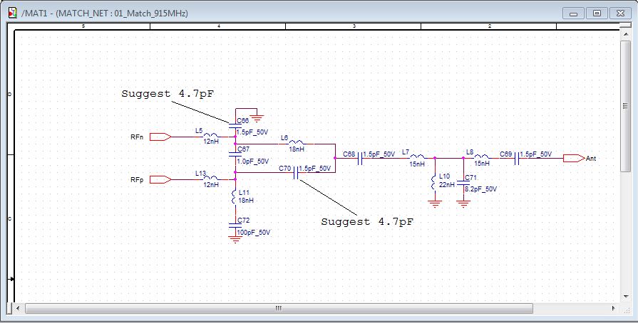
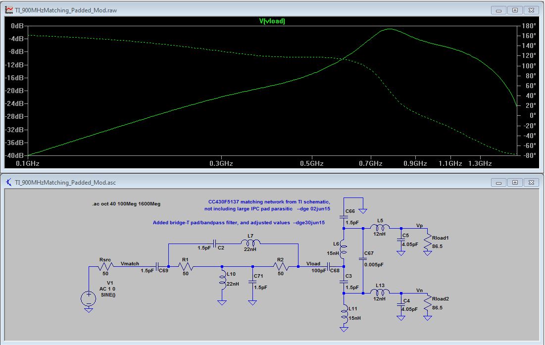
In a SPICE simulation of the balun and matching network, capacitors C66 and C70 provide control of out-of-band response and I replaced these 1.5pF caps with 4.7pF parts. See below.

The RF link now works. However, I still need to open the RX Filter BW to roughly three times the tool (SmartRF Studio 7) recommended value (on the RX side of this unidirectional link). I'm speculating that there might still be a low level oscillation. A sniffer probe on the spectrum analyzer might show this . . .

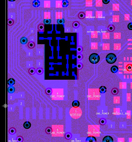
For the next spin of the board, I will reduce the IPC pads to half the area and open windows in the inner two layers (of my 4 layer PWB) to reduce parasitic capacitance. IPC pads for 0402 capacitors measure 27W x 34L mils. (They are sized for manufacturing yield and minimize tombstone failures.) My new pads will measure 27x16mils--still not as small as used by TI, but the pad extension beyond the parts aid hand assembly. As space permits, I will pepper the area around the balun and matching network with as many ground vias as space permits and use poured copper to with multiple vias to ground for connecting the circuit.

It's not clear to me whether TI opened the inner layers on their multi-layer PWB. Any TI RF engineers out there care to weigh in?

  • - Keep the values in the ref design.
    - For a multilayer PCB example, look at the CC1101+CC1190 ref design.
    - What is your stack-up? The most important parameter is the distance between the signal layer and the inner ground layer
    - Not sure where you probe with what and in which state. You will generally not get too much information probing anywhere else than the antenna connector since the impedance of the probe will influence the circuit.
    - Do you know if your software work?
    - If you use a EM as receiver, do you see the RSSI go up when you try to transmit? And the other way, if you send with the EM, do you see a change in RSSI on your board?
  • TER, only after I modified the design was I able to establish communication. However, I will try reversing the modifications and give it another shot. The ground plane on this four layer board is 12mils from the back surface (where the matching network is located). The ground plane is a solid sheet of copper punctured with vias.

    After fighting (this took several days) with the compile and link structure of the Ti examples I'm now able to manipulate the frequency synthesizer and access the registers of the CC1101 module. Aligning the synthesizer frequency to match the TI PWB helped, but the sensitivity is still poor. I stuffed two PWBs, the behavior is similar on both.

    Attached are JPGs of the old and new layouts. Care to critique? I opened the BOTH interlayers on the new layout of this 12-28-12 stackup (the two metal clad 12mil faces are adhered with a 28mil core). 

    DE

    The old (currently in use) layout:

    The new spin:

  • Hi,

    The largest concern with the first layout is there is a large risk of cross talk between the discrete components so the filtering and matching could be effected. This looks better in the new spin version. Do you have any GND plane underneath these components ?

    Regards,

       Richard

  • Richard, thanks for the reply. I think the new layout is better with the ground planes opened up.

    I fired up SPICE and designed the network below. I placed a bridge-T (lossy) matching network between the antenna and the balun. I realize I'm throwing away power with the bridge-T network, but I find that my Tx/Rx is much better behaved--it links immediately and the range is 20 fold when compared to the earlier version with the 4.7pF caps--a change I found necessary to make the link work at all. See earlier posts on squelching oscillation. I restricted my component values to those previously recommended by TI. In the new network, C67 is only a placeholder, it was removed. C2 bridging the 50ohm resistors was stood on end and L7 soldered to the free end. A #34 wire connects L7 to the far end of R2.

    With this change I can continue development without immediately spinning the layout.

  • P.S. The value to the right of L5 and L13 are used to simulated the impedance of the TI CC1101 module. They are not part of the external network. Not shown is C72, the DC blocking capacitor on L11. It's needed so the TI module biases correctly.

    DE