Hello,
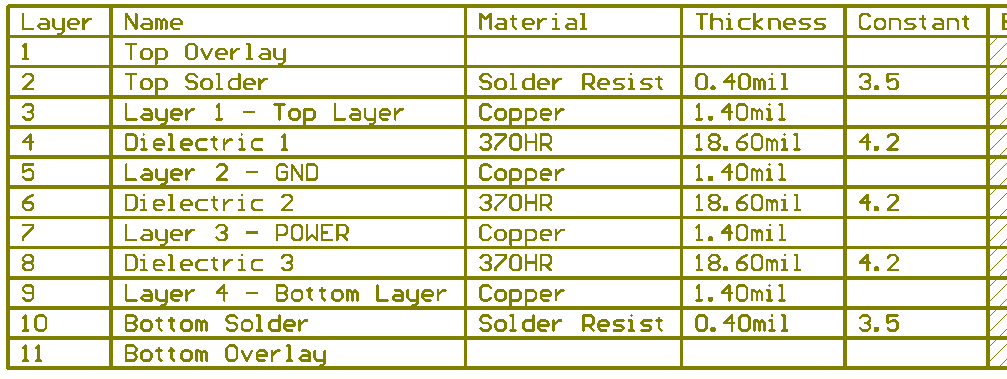
In the TIDA 00484 reference design, the thickness of PCB required for manufacturing seems to be 1.6mm based on the PCBdoc file provided (this is what is written in the table on the right side of the page), while if you sum up the layers of the stack manager it provided 0.85mm... is there any mistake here or do I miss something ?