Hi,
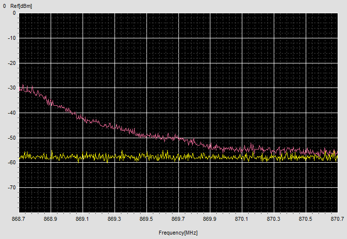
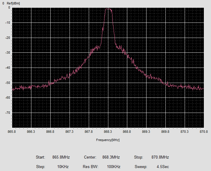
I am developing a CC430F5137 based RF product but I found the RF signals at the side of the spectrum chart is too high.
Please advise.
Thanks a million.
-derong
dyuan@seabreeze.ca
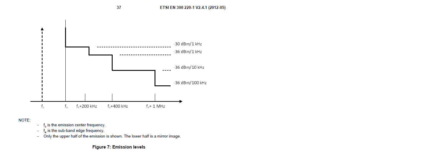
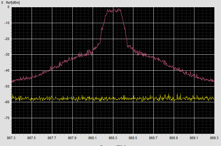
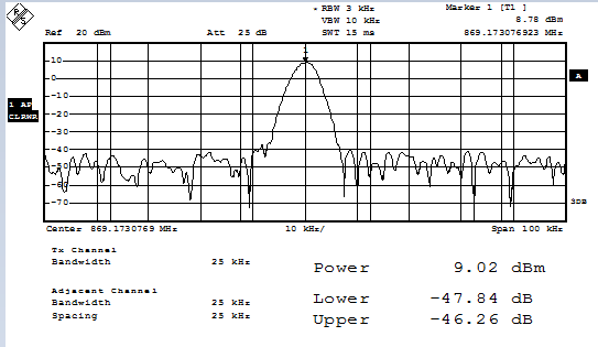
The picture below is the RF spectrum chart.
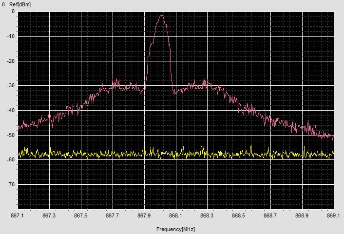
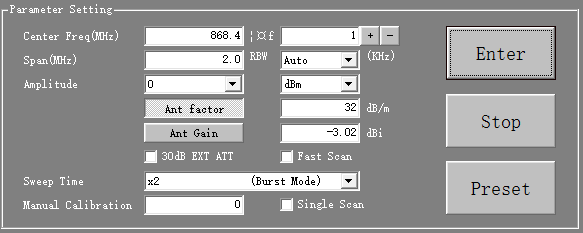
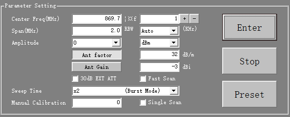
Below is the RF settings and part of the code.
//// Modulation = 2- GFSK
//carrier frequency = 868.3mHz
//deviation =50khz
//receiver channel filter band width =464kHz
//xtal freq =26Mhz
//data rate =175kBaud
//optimized for sensitivity
RF_SETTINGS rfSettings = {
0x0c, // FSCTRL1 Frequency synthesizer control.
0x00, // FSCTRL0 Frequency synthesizer control.
0x21, // FREQ2 Frequency control word, high byte.
0x65, // FREQ1 Frequency control word, middle byte.
0x6A, // FREQ0 Frequency control word, low byte.
0x3c, // MDMCFG4 Modem configuration.
0xb9, // MDMCFG3 Modem configuration.
0x13, // MDMCFG2 Modem configuration.
0x22, // MDMCFG1 Modem configuration.
0xF8, // MDMCFG0 Modem configuration.
0x00, // CHANNR Channel number.
0x50, // DEVIATN Modem deviation setting (when FSK modulation enabled).
0x56, // FREND1 Front end RX configuration.
0x10, // FREND0 Front end TX configuration.
0x30, // MCSM1 Main Radio Control State Machine configuration 1.
0x00, // MCSM0 Main Radio Control State Machine configuration.
0x1D, // FOCCFG Frequency Offset Compensation Configuration.
0x1C, // BSCFG Bit synchronization Configuration.
0xC7, // AGCCTRL2 AGC control.
0x00, // AGCCTRL1 AGC control.
0xB0, // AGCCTRL0 AGC control.
0xEA, // FSCAL3 Frequency synthesizer calibration.
0x2A, // FSCAL2 Frequency synthesizer calibration.
0x00, // FSCAL1 Frequency synthesizer calibration.
0x1F, // FSCAL0 Frequency synthesizer calibration.
0x59, // FSTEST Frequency synthesizer calibration.
0x81, // TEST2 Various test settings.
0x35, // TEST1 Various test settings.
0x09, // TEST0 Various test settings.
// 0x47, // FIFOTHR RXFIFO and TXFIFO thresholds.
0x40, // FIFOTHR RXFIFO and TXFIFO thresholds.
0x29, // IOCFG2 GDO2 output pin configuration.
0x06, // IOCFG0 GDO0 output pin configuration. Refer to SmartRF?Studio
// User Manual for detailed pseudo register explanation.
0x04, // PKTCTRL1 Packet automation control.
0x04, // PKTCTRL0 Packet automation control.
0x00, // ADDR Device address.
0x05 // PKTLEN Packet length.
};
main()
{
// Initialize I/O ports and set up port mapping
.......
//------------------------------------------------------------------------------
//reset the PATABLE value
PATABLE_VAL = 0x50; // 0XC4-- 10 dBm;
// 0X50-- 0 dBm;
// 0X2D-- -6 dBm;
// 0X26-- -12dBm;
// 0x05-- -30dBm;
// 0xc0-- max
//ResetRadioCore
// Strobes SRES -> sets radio in SLEEP mode
Strobe(RF_SRES);// Reset the Radio Core
Strobe(RF_SNOP);// Reset Radio Pointer
//InitRadio
// Set the High-Power Mode Request Enable bit so LPM3 can be entered
// with active radio enabled
PMMCTL0_H = 0xA5;
PMMCTL0_L |= PMMHPMRE_L;
PMMCTL0_H = 0x00;
WriteRfSettings(&rfSettings);
WriteSinglePATable(PATABLE_VAL);
// Set up SYNC WORD
WriteSingleReg(SYNC1, SYNC_WORD_MSB);
WriteSingleReg(SYNC0, SYNC_WORD_LSB);
//change FIFO_THR back to 0x40
WriteSingleReg(PKTCTRL1, (rfSettings.fifothr & 0xF0));
state = STATE_SLEEP;
//------------------------------------------------------------------------------
/* MCU clock system (UCS) initialization
* - Start the 32768Hz crystal oscillator XT1
* - Configure the FLL to generate 8MHz clock using XT as reference
* - MCLK = SMCLK = 244 * fXT1 = 7.995392MHz from DCO/2.
*/
UCSCTL3 |= SELREF_2; // Set DCO FLL reference = REFO
UCSCTL4 = SELA_2+SELS_3+SELM_3; //ACLK = REFO, MCLK=SMCLK=DCOCLK.
UCSCTL6 = XT2OFF & msk_1 | //XT2 is off
XT1OFF & msk_1; // XT1 is Off
__bis_SR_register(SCG0); // disable FLL pulling of DCO
UCSCTL0 = 0x0000; // set DCO to lowest tap
// FLL loop divide-by-2, Fsys/Fxt1 ratio = 243+1 = 244
UCSCTL2 = FLLD__2 | 243;
UCSCTL1 = DCORSEL_5; // good for 10..20MHz, we run Fdco = 16MHz and divide
// by 2 to make sure that clock duty cycle = 50% since
// we run at the 8MHz max limit for PMMCOREV = 0.
__bic_SR_register(SCG0); // re-enable FLL control
// maximum FLL settling delay = 1024 * f_MCLK / f_FLLREF
__delay_cycles(250000lu);
bTimeout = 100; // try max 100ms
// wait for ALL oscillator fault flags to become clear
while (SFRIFG1 & OFIFG)
{
__delay_cycles (8000lu); // delay ~1ms
// clear individual flags
UCSCTL7 &= ~(XT2OFFG + XT1LFOFFG + XT1HFOFFG + DCOFFG);
SFRIFG1 &= ~OFIFG; // clear sum flag
if (--bTimeout == 0)
{
//something wrong
SOFTWARE_BOR_REBOOT
}
}
UCSCTL4 = SELA__XT1CLK + SELS__DCOCLKDIV + SELM__DCOCLKDIV;
//Initialize timers/counters
.......
//Initialize some variables
......
// the following code is used to transmit RF signals only
while(1)
{
CLRWDT_16s
TxBuffer[2] = miniFriend_1;
TxBuffer[3] = miniFriend_2;
TxBuffer[4] = miniFriend_3;
TxBuffer[5] = RF_BUTTON;
RF_Transmit(20); //issue alarm 10s
}
// the function below is to be called by the main() function above
void RF_Transmit(unsigned char time)
{
unsigned char i;
CLRWDT_16s
PATABLE_VAL = 0xc4; // 0XC4-- 10 dBm;
// 0X50-- 0 dBm;
// 0X2D-- -6 dBm;
// 0X26-- -12dBm;
// 0x05-- -30dBm;
// 0xc0-- max
WriteSinglePATable(PATABLE_VAL);
g_qHalfSecTick =time;
while(g_qHalfSecTick)
{
for(i=1;i<3;i++)
{
CLRWDT_16s
TxBuffer[0] = TxBuffer[i*2];
TxBuffer[1] = TxBuffer[i*2+1];
Strobe(RF_SIDLE);
Strobe(RF_SFRX);
Strobe(RF_SFTX);
Strobe(RF_SCAL);
while ((Strobe(RF_SNOP) & 0xF0) != 0x00 );
state = STATE_TX;
// Set up 2 preamble bytes
WriteSingleReg(MDMCFG1, (rfSettings.mdmcfg1 & 0x8f));
// Set up 16 bit sync word (16/16)
WriteSingleReg(MDMCFG2, (rfSettings.mdmcfg2 & 0xf4) | 0x02);
// Disable CRC at end of packet
WriteSingleReg(PKTCTRL0, (rfSettings.pktctrl0 & ~0x04));
//disable appending RSSI and LQI info at the payload
WriteSingleReg(PKTCTRL1, (rfSettings.pktctrl1 & ~0x04));
// Stay in TX (send preamble) after finishing packet transmission
WriteSingleReg(MCSM1 , (rfSettings.mcsm1 & 0xfc) | 0x02);
RF1AIES |= BIT9;
RF1AIFG &= ~BIT9; // Clear pending interrupts
RF1AIE |= BIT9; // Enable TX end-of-packet interrupt
// The packet length is the complete TxBuffer
TxBufferLength = 2;
// Set up packet length
WriteSingleReg(PKTLEN, 2);
WriteBurstReg(RF_TXFIFOWR, TxBuffer, TxBufferLength);
Strobe( RF_STX );
T_LEARN =3; //1.5s
while(T_LEARN >0)
{
if (state != STATE_TX)
{
break;
}
}
}
}
PATABLE_VAL = 0x50; // 0XC4-- 10 dBm;
// 0X50-- 0 dBm;
// 0X2D-- -6 dBm;
// 0X26-- -12dBm;
// 0x05-- -30dBm;
// 0xc0-- max
WriteSinglePATable(PATABLE_VAL);
}