This thread has been locked.

If you have a related question, please click the "Ask a related question" button in the top right corner. The newly created question will be automatically linked to this question.

CC1310 868MHz RF frontend design

Other Parts Discussed in Thread: CC1310

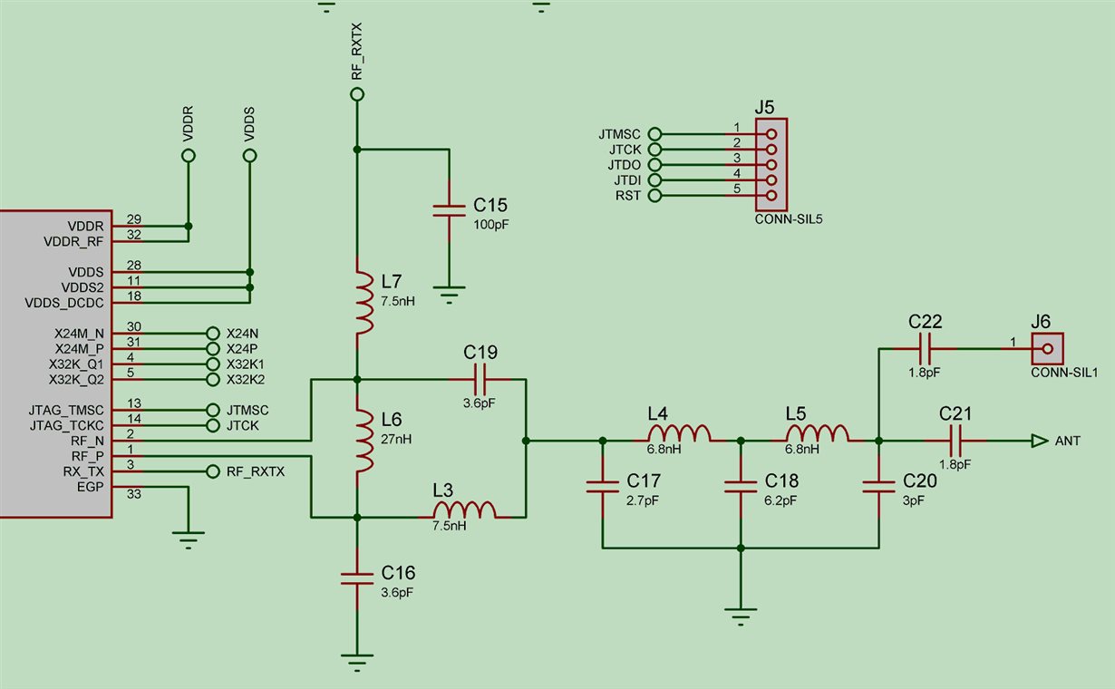
Hi everyone. I am currently working on integrating cc1310-based 802.15.4 radio into some device. Before integrating this into device I tried to develop PCB, based on launchpad design. Anyway after mounting board, the signal I measured was pretty lower, then the signal, emitted by cc1310 launchpad. My RF frontend looks like this:

I havent found any 7.5 nH inductors in local stores, so I replaced it with 6.8 nH. Asking for any help and critics regarding my design. Another question is how should I change my circuitry, if I want to use simple dipole antenna. Regards, Vadim.

  • Please follow the reference design.
    - the balun L3, C16, C19, L7 should be symmetrical w.r.t RFN and RFP. In your layout there is no symmetry and you will get phase and amplitude imbalance.
    - the LC filter has not been laid out properly. Ground connection for C17 and C20 for instance is poor as they share the same connection to GND (each and every capacitor should have a separate via to ground)
    - use the recommended component values
    - have you disconnected the PCB antenna when measuring the conducted output power using J6 connector? (i.e. remove C21)
    - there are no impedance matching components connected to the PCB antenna. This needs to be fixed in next revision
  • Sverre said:
    have you disconnected the PCB antenna when measuring the conducted output power using J6 connector? (i.e. remove C21)

      Yes, I had.

    Due to lack of experience with RF circuits I considered using Johanson IPC in next revision, as described in swra524. I have a question(1): what is the purpose of LC filter C12 - C14, L13 , L14, is it for antenna matching?


    Sverre said:
    there are no impedance matching components connected to the PCB antenna. This needs to be fixed in next revision

    As I mentioned, I am not experienced enough in RF circuits design, (question 2)may I just use antenna matching components, as described in chapter 4.2.1.2 of swra227e? Another confusing thing is absence of some components for antenna matching on my launchpad. What should I read or calculate, if I want to use monopole antenna  instead of PCB antenna(3)? 

    Another question(4) is: are there any "load" capacitors required for use with 24MHz oscillator (usually there are two capacitors, connected between quartz outputs and ground). I suppose to use Geyer KX-7T or KX-KT crystals for my design. And the last question(5): what is the best strategy of placing vias on PCB ground polygon, where may I read about it?.

    Sorry for my incompetence. Regards, Vadim Mischuk.

  • Q1: C12 - C14, L13 , L14 are impedance matching and filtering. Antenna matchig has to be placed after C15.

    Q2: On the LP the only antenna matching needed is the serial cap shown between the two black rings in the picture. The matching will be dependent on the size of your board and the casing (plastic can shift the resonance frequency a fair bit) so in effect you have to measure on your design.

    Q4: CC13xx has build in load caps, see processors.wiki.ti.com/.../CC26xx_Tips_and_Tricks for how to adjust them.

    Q5: Always place 1-3 vias close to a ground pad. Other than that, place vias to ensure you have best possible connection between the ground layers.