This thread has been locked.

If you have a related question, please click the "Ask a related question" button in the top right corner. The newly created question will be automatically linked to this question.

CC1310 Single-ended Operation

Other Parts Discussed in Thread: CC1310, CC1350, CC-ANTENNA-DK2, CC1350STK

I am having a little trouble finding information and/or reference designs based on single-ended operation.

I am looking to create a solution that uses 2 FEMs operating in 434MHz and 900MHz. It appears that a single-ended approach might be a simpler solution than switching the differential signals and having separate baluns and matching networks for each RF path.

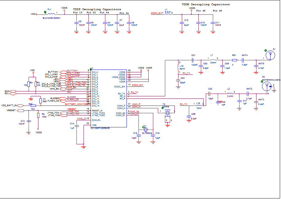
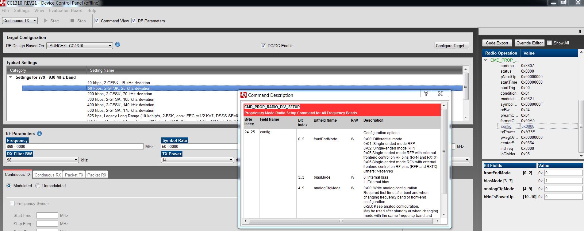
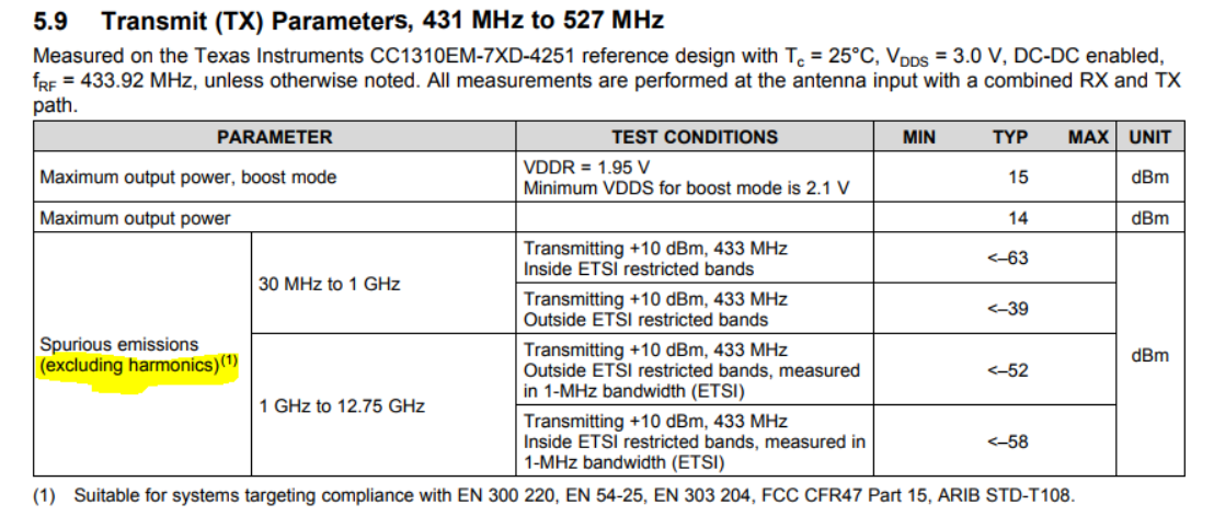
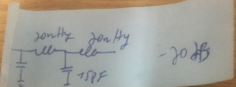
I have some questions from the datasheet SWRS181C on page39 (of course with my annotations):

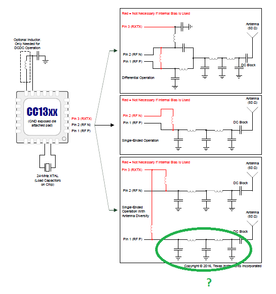
  1. When the CC1310 is operating in single-ended mode are the RF inputs/outputs internally match to 50 0hms?
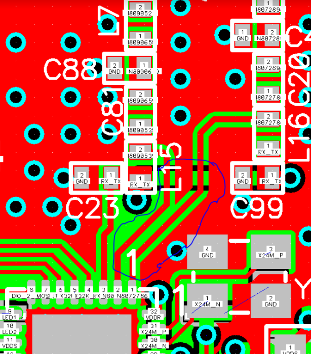
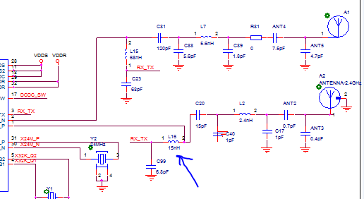
  2. What is the purpose of this LC network in seen in the datasheet, matching, filtering? Is there information on calculating these values for single-ended operation?
  3. Can you briefly explain (in laymans terms) the purpose of the RXTX pin, it provides a bias to the circuit but how does that improve the receiver sensitivity 1dB as stated in the datasheet?

Any other comment would be welcome.

Thanks,

Gary

  • Hi Gary,

    For a single-ended ref design, the CC1350 SensorTag is available. This operates at 868/915 MHz and 2.4 GHz.

    1. The RF_P and RF_N ports are not 50 ohms but the external passives provide a 50 interface and low-pass filtering.
    2. This is a low-pass filter network. This is mainly to limit the harmonics below the regulation level set by ETSI/FCC.
    3. RxTx is a port that provides external biasing to the internal LNA. Biasing can be configured as external or internal. For optimum performance, external biasing should be used.

    Regards,
    Richard
  • Hi Richard,


    Thanks for the reply and information, I have looked at the CC1350 reference but I am still not able to determine the values necessary for the external passives at 434 MHz.

    I have also looked at the CC-Antenna-DK2 documents, but again I am at a loss on how to calculating the values of the external passives based on the CC1350 reference design.

    I will plan on using the external biasing; but have the following questions:

    1. Is there an optimal impedance for the RF_P and RF_N ports that your using to create your matching network?
    2. Could you provide initial values for the external passives to operate at 434 MHz? 

    Thanks in advance.

    Gary

  • Hi Gary,

    For 433 MHz and 2.4 GHz single-ended configuration, please see attached schematic as a guide for the values to use:

  • Thanks you.
  • Hi Gary, Just to be clear that we have not finished this design yet so this is an early guide to the values that should be used.
  • HI Richard,

    Understood, I know the silicon rev B is newly released and will support 434MHz operation.

    I was looking for a starting point for schematic capture and layout and have the reasonable expectation of needing to tune/change component values as we move through the process. From a timeline standpoint I am looking to create a prototype board in early January.

    Do you feel that filter design is sufficient at this stage in the design and only the component values would change moving forward?
    Do you have a idea when your design might be finalized?

    Gary
  • Hi,
    The filter design should be sufficient and it should just be the component values which can change. We do not have a date when this particular design will be finalized.
    //Richard
  • Hi Richard,

    I want to use 434MHz and 2.4GHz design for cc1350. I have seen that optimal differential impedance of RF output is 33+j15 for 433MHz.

    Also frequency of 44+j15 impedance, which is stated on datasheet section 7, is not obvious.

    Why we use 50ohm impedance for single ended design, is there any extra calculation of pin impedance for single-ended operation? Could you please provide some information about this?

  • Hi Richard, We followed the single ended reference for 433.9Mhz on cc1350. On Spurious emission testing, we see that the third harmonic exceeds limits. Could you please suggest how to fix this? Should we try different frequencies? Or do we have to replace components on the LC network? Thanks a lot, YTE
  • The schematic Ricard provided was a untested suggestion. From your findings it sounds like you have to design the filter slightly differently with more attenuation on the harmonics.

    How high output power are you allowed to use on 433.92 MHz where you want to use the product?
  • Hi TER,

    We will need to use the product in Israel, Europe and in the US, so FCC and CE.
    In Israel we use the device maximum power - 14db.
    for CE and FCC,we plan also to use maximum power.

    from measurements we get 88uV/M tested from 3M.

    1. for CE requirement for 433.9 is 10mw, which is equivalent to 107uV
    2. For FCC limits are in 200 uV/m from 3 meters, so we should be fine there too.

    Thanks,
    YTE

  • 10 mW converted to dBm: 10 log(10 mW/1 mW) = 10 dBm

    The harmonics when operating under FCC 15.231 at 433 MHz only needs to be at -20 dBc since they do not fall in restricted bands (true for 2nd to 5th at least when operating up to 433.33 MHz). Furthermore, the output power is limited to -14.4 dBm under 15.231a (simple control operation, no periodic transmission) and -22.4 dBm under 15.231e (other than simple control application). The output power can be increased by up to 20 dB if the transmission lasts less than 100 ms; 20log(TX-on time/100 ms). Maximum output power under 15.231a is thus +5.6 dBm.  

  • Hi TER,

    We are limited  to 107 uv/M according to CE regulations (EN 300 220)

    On tests re saew 87 uv/M, so we are bellow limit.

    However, connecting the probe after C14 we see high power on the third harmonic (1.3Ghz), as high as the 433.92, is this reasonable?

    Attached is our SmartRF settings.

    we use cwTaskFunction (unmdulated) from the rfCarrierWave_CC1350STK_TI example. for this test.

    smartrf_settings.rar

  • Is this measurement done conducted?

    Looking at your settings it looks like you use max output power and then I would expect a higher fundamental . It looks like the level of the 2. harmonic is low (in the noise floor) but the 3. harmonic is higher than the fundamental which doesn't make sense.

    Do you use 433 MHz + 2.4 GHz? If so, does the 2.4 GHz path give expected values both for the fundamental and the harmonics?
  • Yes, it is done conducted. measured after C14 and before Ant4 and Ant5.
    We will check the 2.4 Ghz harmonics.

    Can you take a look at the smartrf configuration?
    Maybe something in the configuration isn't right (like configuration/bias etc).

    Thanks,
    YTE.
  • When you measure after C14 you disconnect Ant4 and ant5 I assume? 

  • Yes, Ant4 and Ant5 are disconnected.

    See bellow the results for the 2.4Ghz.

    from technical reasons, we connected the probe before the printed antenna (after Ant2 and Ant3), so maybe it is not the most accurate.

    We can see the second harmonic is pretty high, is this an expected behaviour for this design (CC1350_STK)?

    can this help us understand the high 3rd harmony in the 433Mhz?

    Thanks,

    YTE.

  • To avoid confusion, could you post a picture of how/ where you measure?

    Have you done the same measurements on a unmodified CC1350 STK? (both 868 MHz and 2.4 GHz is of interest)
  • Hi TER,

    Attached a photo for how we connected the 433Mhz (we don't have a picture from the 2.4Ghz, but it is just before the printed antenna.

    We don't have a working sensortag to test.

    we have made a filter to reduce the third harmony, and it seems to work.

    Question is if it should have been so high in the first place, and if the power of our signal at 433, is as exppected:

    87uv/M measured from 3 Meters, configured to 14DB.

    Or power should have been much higher?

    Thanks,

    YTE.

  • Btw, do you have a schematic you can share?

    On the picture ant4 and ant5 looks to be mounted?

    What I see of the layout on the picture is that the filter does not have optimal layout. When all the caps to ground goes to the same side part of the signal can bypass part of the filter. If you take a look at our reference designs the caps to ground in the match/ filter every second one are always rotated 180 degrees.

    Do you have the conducted version of "87uv/M measured from 3 Meters, configured to 14DB."? It's easier to compare conducted numbers in dBm.
  • Hi TER,

    Bellow is the Original Schematics, filter is based on 868 ref design.

    We replaced the bellow components to fit the 433 ref design:

    L15 - 68nh --> L15 220nH (0402)
    C81 - 120pf --> C14 330pf (0402)
    C88 - 5.6pf --> C12 4.7pf (0402)
    L7 5.6nH --> L13 20nH (0402)
    C89 1.8pf --> C13 12pf (0402)
    Ant4 7.5Pf --> L14 20nH (0402)
    C23 - 68pf --> C23 330pf (0402)

    Ant4 and Ant5 are assembled, but disconnected from prob. 
    R81 was dissasembled and prob is connected to a single pad of the R81.
    Attached is the layout, RF path was supposed to be exactly the same as CC1350_STK. 
    Can you please specify the components that are not the same as the reference? 
    The "87uv/M measured from 3 Meters, configured to 14DB" was done in an RF shielded room in a test lab for CE standard, they do not make conducted testing.
    We made a conducted test were we saw the high 3rd harmony, sent earlier.
    Thanks,
    YTE
  • Hi TER,

    We are still Struggling with the third harmonic (for 433Mhz) issue.
    Something seems weird in the behaviour, and i cannot find the root cause.

    We have prepared 3 different boards with filters on the sub-1g end to reduce the third harmonic by 20db, 30db and 40db.
    We have tested the filters (conducted) and results seemed as expected.

    When tested in laboratory, for the spurious emmision standard test, we saw third harmonic was still high, and filters seemed to have little affect.

    We kept on debugging, to understand were this frequency is comming from.

    we found out the following:

    1. RF_N and RF_P both put out the same level of 433.92MHZ signal. RF_P is on the BLE antenna path and we didn't expect it to have any output (is this assumption correct?)

    2. When removing components from the BLE Path we saw the third harmony signal going down (tested from air).

    SmartRF is configured to single ended, where 433Mhz is configured to the RF_N, and 2.4Ghz to the RF_P.

    Trying to reduce the TXPower from S/W (using EasyLink_setRfPwr), seemed to have little/none affect, even when reduced from 13 db to 0 and -10.

    We suspect that the RF core is not configured according to the smartrfsettings configuration.

    Is there a way to check the rf registers directly?


    Thanks
    YTE
  • It seems like the 3rd harmonic of 433 MHz is leaking over to the 2.4 GHz path. Can you add a 1.3 GHz notch on the 2.4 GHz path to see if this helps.
  • Thanks Richard,

    we will check.
    What about the fact that both RF_N and RF_P both put out the same level of 433.92MHZ signal? is that an expected behaviour on a single ended configuration?

    We want to be sure that the core isn't configured as differential.
    We are also disturbed by the fact that power configuration change on easylink doesn't have any affect on the output power.

    what is the way to verify that easylink configured the rf core propperly?
  • Hi,

    The output power should not be the same level at both RF_P and RF_N if single-ended is chosen.

    The RF front end can be configured  in SmartRF studio:

  • Thanks Richard,

    So to make sure, our design is as attached  (based on cc1350STK).

    for the A1 antenna (433Mhz), we should configure the config bits to  0x02 or to 0x05?

    Should the biasMode be set to 0x0 or 0x1?

    Thanks,

    YTE.

  • Hi Richard,

    So our original front-end configuration is 0x2(single ended rf_n) , and bias mode is 0x1 (external bias).
    Still, we see the same signal power on both rf_n and rf_p (433.92Mhz).

    also, changing the power level doesn't seem to affect the signal.
    BTW - why on smartRf 433 configuration, power can only be changed between 6-14db, where in 868 power can be set to -10db?

    We are really frustrated from this issue, after months of debugging, we still cannot certify the board, or get a clue about the root cause.

    Thanks,
    YTE
  • Hi Richard,

    So changing the filter on the BLE path helps in reducing the 3rd harmonic (1.3Ghz) from the Sub-1G path.

    But we are still disturbed from the fact that both rf_n and rf_p produce +- the same power level of 433Mhz, although configuration is single ended (and not differential).

    Still not sure if this is an expected behaviour.

    Measuring poth pins while only one of it is transmitting, what should we expect to see from the not transmitting pin, how many db less ? (not looking for an accurate answer, just what you think is reasonable).

    We use the sensortag cc1350 as reference, which is planned for 868/915Mhz, and we use it for 433Mhz, do you think it could make it easier for the signal to leak between rf paths?

    Could this be related to layout issues (pcb depth, close paths etc.)?, i attach gerber files and appreciate if you could have a look.

    also bellow is a general view:

    Thanks a lot,

    YTE

     CC2640-N_GBR.zip

  • Hi Richard/TER,

    We are still trying to pass the spurious emission test.
    The 433 filter reference is a 3 level filter, while our design (based on 868Mhz) is a 2 level filter.
    So when replacing the components from the original cc1350STK design to the 433Mhz design, we didn't add the antenna matching components as we didn't have place in the layout.

    Few questions:

    1. If antenna matching is not good, should this have significant affect on spurious emission (specifically 3rd harmonic 1.3Ghz)?
    2. If antenna matching is not good, could this be related to the fact that we see both RF_N and RF_P put out the same level of 433.92MHZ signal? (remind that front end is configured for single ended)
    3. We are using TPS70930DBVR , for reduce voltage from 9V to 3.3V. could this device be a source for 1.3Ghz?


    Thanks,
    YTE
  • Hi,

    We have made progress in understanding in the spurious emmision issue, and could use some advise.

    1. we have made conducted measurements, at end of filter not including antenna and matching components and saw 3rd harmonic (1.3Ghz) at -25dbm.

       We checked it also on TI cc1350 sensortag and got -19dbm.

       The 3rd harmony of the cc1350 seems to be very high!

       From some reason, harmonies power is not mentioned in the datasheet for 433 (although it is mentioned for other frequencies):

    2. After severall filters didn't solve the problem (we even tried -40db filter on the 433 path), we started looking for other contributors.

    3.testing with spectrum analyzer, we got to the conclusion that the a significant part of the 1.3 Ghz is leaking from the 433Mhz Path to the 2.4 Path around the marked area in the layout (another option is that processor itself outputs 1.3Ghz on the 2.4 Path):

    4. All tests we have made are attached. Note that all tests done conductive and without connecting ground to spectrum. however it is accurate enough to approve our assumption.

    5. We think to continue in two directions, and would advise from TI experts:

         a. change the filter on the 2.4 path to reduce 1.3Ghz --> not sure if it would be effective enough...

         b. change layout to assure 1.3Ghz doesn't leak --> unless we will find out that the problem is in the processor itself, and than it will not help, please advise.

    Thanks,

    YTE

    Tests results debugging spurious.xlsx

  • To get a highly efficient PA the 3. harmonic goes up.

    The assumption is that the 3. harmonic leaks from RF_P to RF_N (or the other way) internally in the chip and to avoid issues:
    - Use a RF switch on the path with the highest frequency to increase isolation.
    - Or, implement a notch on the path with highest frequency to filter out the harmonic.
    - Or, use differential design.
  • Thanks TER,

    We will try implementing a notch on the 2.4 Path, we prefer not to relayout the pcb.

    We saw on simulation that by replacing L16 on the 2.4 path from 15nHy to 2.2nHy, we reduce 30db on 1.3Ghz, and gain 2.5db on 2.4Ghz:

    We are assuming that the RX_TX path has high impedance, does it?

    if not, can you recommend a better filter for the 2.4?

    for the 433, to reduce 1.3Ghz,we replace inductors by 15nHy, and capacitors by 15pf, simulation shows -20db:

    If you think it makes sense, we will check it conducted, and return to lab for spurious emission testing.

    Thanks,

    YTE