This thread has been locked.

If you have a related question, please click the "Ask a related question" button in the top right corner. The newly created question will be automatically linked to this question.

RTOS/CC1310: CC1310 - Controlling External LNA/PA with DIOs

Part Number: CC1310

Tool/software: TI-RTOS

Hi all,

We are designing a gateway that has external front-end module. So we need to activate external LNA and PA during transmit and receive processes. For this, we used RF Core Data Signals to activate external LNA and PA according to SWCU117F document section 11.3.2.1. 

We assigning these signals (RFC_GPO0 and RFC_GPO1) to DIOs. The code is shown below.

PIN_Config paTable[] =

    {
    Board_pa_CSD | PIN_GPIO_OUTPUT_EN | PIN_GPIO_LOW | PIN_PUSHPULL | PIN_DRVSTR_MIN,

    Board_pa_CPS | PIN_GPIO_OUTPUT_EN | PIN_GPIO_LOW | PIN_PUSHPULL | PIN_DRVSTR_MIN,

    Board_pa_CTX | PIN_GPIO_OUTPUT_EN | PIN_GPIO_LOW | PIN_PUSHPULL | PIN_DRVSTR_MIN,

    PIN_TERMINATE

    };

void initPowerAmp(void)
{
    paHandle = PIN_open(&paState, paTable);

    PIN_setOutputValue(paHandle, Board_pa_CSD, Board_LED_ON);

    PINCC26XX_setMux(paHandle, PIN_ID(Board_pa_CTX), 0x30);
    PINCC26XX_setMux(paHandle, PIN_ID(Board_pa_CPS), 0x2F);
}

With these piece of code, RF Core signals can be able to control external LNA and PA. But there is a problem about it. Although i am sure that my code works and sends data, sometimes data can not be sent .

For example, after i sent 64 piece of data from CC1310, i could just observe 58 piece of data in air. Also after changing operation frequency data miss rate is incresing.

So i thought that RF core signals can not control external LNA and PA properly. What is the problem about that in here?

Best regards.

Ramazan

  • Hi,

    there are many customers using those signals and I have never heard that they are not working properly. How often does this happen? How do you check how many symbols are sent on air? Which part of the transmission is missing? Are you sure that the front-end is working correctly?

    You can double-check what goes out on air by observing the MCE_GPE0 signal as described here and here. MCE_GPE0 shows the data that goes to the modulator.

  • Hi Richard,

    In my scenario, when transmiting packets,
    Board_pa_CTX = 1,
  • Hi Richard,

    In my scenario, when transmiting packets should be,
    Board_pa_CTX = 1, Board_pa_CPS=0


    So when packet transmitting, while CC1310 makes RFC_GPO1 "1" , does it also make RFC_GPO0 "0" ?

    Because when i set these pins 1 and 0 as hard coded, transmission is achieved.

    Regards.

    Ramazan
  • Yes, CPE_GPO0 (LNA) and CPE_GPO1 (PA) are never enabled at the same time. But the timing is much tighter as when you set the outputs from your application. I am afraid, I can't provide more support here. Unless you can proof that those signals do not behave as expected, I have to refer you to your front-end. Does it really meet the timing characteristics of the CC1310? What front-end are you using?
  • Ramazan: Have you measured the length of the PA_EN/ LNA_EN signal and compared them with the packet length?
  • Hi,

    SE2435L is the front-end module that we used in design. 

    It is said that in datasheet : Fast turn-on/turn-off time: < 1 μsec.

    CC1310 sets RFC_GPO1 signal before transmission. For example, i transmit one packet and CC1310 sets RFC_GPO1 signal. Will CC1310 change this signal from "1" to "0" until next transmission ?(i assume we wont change the radio mode from transmit to receive) 

    So does CC1310 change these signals as arbitrary except transmitting and receiving time?

  • Hi TER,

    I did not measured length of these signals yet. I will look at it in tomorrow and turn back to you with an answer.

    Regards.

    Ramazan
  • Hi,

    We solve the problem. We powered new designed board from JTAG. When i power device from battery it works as expected. But i have a question about signals.

    Can we control these RFC_GPO0 and RFC_GPO1 signals' timing? ( For example, if i want can i arrange RFC_GPO1 to set 5 microseconds before transmitting?)

    Regards. 

    Ramazan

  • The RFC_CPO signals comes directly from the RF core and the timing is fixed and set to give lowest possible power consumption. Why do you want 5 us extra? To add more time you can send longer preamble.
  • Hi,

    I just wanted to learn its timing behavior. CC1310 already has taken into account power consumption. Thank you for your answers.

    Best regards.

    Ramazan

  • Hi:
    I also have a problem related to the RFC_GPO0 signal. In my application, I need to control other three switch while using the PA or LNA. So I maps the RFC_GPO0 signal to an appointed pin and then capture this pin's level, but it seems anything wrong since it doesn't work as what I designs.
    My code is as follows:

    static PIN_Config palnaPinTable[] =
    {
    CTRL_LNA_EN | PIN_GPIO_OUTPUT_EN | PIN_GPIO_LOW | PIN_PUSHPULL| PIN_IRQ_BOTHEDGES, /* LNA Off by Default */
    CTRL_PA_EN | PIN_GPIO_OUTPUT_EN | PIN_GPIO_LOW | PIN_PUSHPULL| PIN_IRQ_BOTHEDGES, /* PA Off by Default */
    PIN_TERMINATE /* Terminate list */
    };
    void Board_Palna_initialize(uint32_t hgm)
    {
    if(!pinHandle)
    {
    pinHandle = PIN_open(&pinState, CTRLPinHandleTable);
    if(!pinHandle) {
    System_abort("Error initializing board LED pins\n");
    }
    }

    if (!palnaPinHandle)
    {
    /* Open PA/LNA PIN driver */
    palnaPinHandle = PIN_open(&palnaPinState, palnaPinTable);

    /* Set IO muxing for RFC GPOs */
    PINCC26XX_setMux(palnaPinHandle, CTRL_LNA_EN, IOC_PORT_RFC_GPO0);
    PINCC26XX_setMux(palnaPinHandle, CTRL_PA_EN, IOC_PORT_RFC_GPO1);
    PIN_registerIntCb(palnaPinHandle, &CTRL_TxRx_Switch);
    }

    }
    void CTRL_TxRx_Switch(PIN_Handle handle, PIN_Id pinId) //(uint8_t mode)
    {
    if(PIN_getOutputValue(CTRL_PA_EN)== 1)//if(mode == RF_TRANSMITTING)
    {
    //sw2[v1 v2 v3]= [0 0 1] --> transmit
    PIN_setOutputValue(pinHandle, CTRL_SW2_V1, 0);
    PIN_setOutputValue(pinHandle, CTRL_SW2_V2, 0);
    PIN_setOutputValue(pinHandle, CTRL_SW2_V3, 1);
    }
    else if(PIN_getOutputValue(CTRL_LNA_EN)== 1) //receive
    {
    //sw2[v1 v2 v3]= [0 1 0] --> 430~450 receive
    PIN_setOutputValue(pinHandle, CTRL_SW2_V1, 0);
    PIN_setOutputValue(pinHandle, CTRL_SW2_V2, 1);
    PIN_setOutputValue(pinHandle, CTRL_SW2_V3, 0);

    }
    }
    But it seems it doesn't work. I don't know why, can you help me?
  • Well of course, edge triggered interrupts only work on GPIO pins, but you re-mux them to the radio so they're no longer GPIO.

    Use external logic gates to generate your desired signals.

    V1 appears to always be 0 so that's easy. You can route PA_EN to V3 and LNA_EN to V2 to generate the rest of your truth table - however you don't seem to handle the state where the radio is neither transmitting nor receiving.
  • Hi Micheal:
    Thank you for your reply? What can I do if I have to handle the state where the radio is neither transmitting nor receiving, since I have three other switchs and two leds(tx_led and rx_led) to control.
  • Hi summery,

    you can route the same RF core signal to multiple pins:

    PINCC26XX_setMux(ledPinHandle, Board_LED1, PINCC26XX_MUX_RFC_GPO1);
    PINCC26XX_setMux(ledPinHandle, Board_LED2, PINCC26XX_MUX_RFC_GPO1);

    You can also invert the level of certain pins:

    PIN_Config pinTable[] =
    {
        Board_PIN_LED1 | PIN_GPIO_OUTPUT_EN | PIN_GPIO_LOW | PIN_PUSHPULL | PIN_DRVSTR_MAX,
        Board_PIN_LED2 | PIN_GPIO_OUTPUT_EN | PIN_GPIO_LOW | PIN_PUSHPULL | PIN_DRVSTR_MAX | PIN_INV_INOUT,
        PIN_TERMINATE
    };

    With this, you should be able to generate any combination of signals.

  • Hi Richard:
    Thank you for your reply. Well, may be I made a bad description for my application.
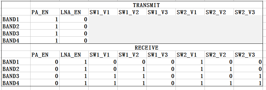
    Actually I need to control the switches according to the state of the RF core, transmitting or receiving, and also need to take the frequency band used into account at the same time. According to the filters parameters, we have divided the application frequency into three bands, the logic of these three switches' level aren't just the same or invert to the RF core signal, So I cannot just only route the RF core signal to these pins, I need to handle the state where the radio is neither transmitting nor receiving. So, how can I do?
  • Hi,
    please create a truth table for all of your signals as Michael has suggested and post it here. Then we can see what is possible.
  • TRUE TABLE:

  • Again you've missed the state where the radio is neither transmitting nor receiving, and I assume the unfilled cells in your transmit table are "don't care" ?

    You could achieve most of that behaviour by re-muxing everything when you change bands.

    SW2_V1 and SW1_V3 never change, so just wire them directly to the relevant power rail.