This thread has been locked.

If you have a related question, please click the "Ask a related question" button in the top right corner. The newly created question will be automatically linked to this question.

CCS/CC1310: Memory Error When Writing to Specific Address During Boot

Part Number: CC1310


Tool/software: Code Composer Studio

Hi,

I've designed a custom PCB using a CC1310F128 IC, and am running into an issue when I try to run my software on it.  I developed the code on a Launchpad, and I've never had issues with it.  Importantly, the issue is happening well before my application code is even called.

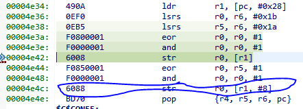
When my PCB resets the CC1310, i can successfully enter the ResetISR, and single step through the boot assembly until I reach the function "NOROM_TrimAfterColdResetWakeupFromShutDownCfg1()".  During this function there's a block of assembly where it tries to write a value to the address 0x43200008, and it causes the debugger to lose control of the core.  I haven't been able to find out what's supposed to be in memory there, or if there's a way around this issue searching the forums.

Here's the block of assembly, and the resulting error.

Any help would be enormously appreciated,

JS

  • Hi Joseph,

    What JTAG connection are you using to debug your IC? And are you sure address 0x43200008 is accessed? Would appreciate it if you supplied a screenshot of the CPU registers as well at the same debug point.
  • If you run the code on the LP, are you able to do exactly the same single stepping without issues?

    What is the delta between the LP and your board? (what is different)
  • I'm using the XDS110 from one of the Launchpads I have laying around.  Here's a screenshot of the CPU registers on the exact instruction that fails.


    and this is what we see on the Launchpad:

    I'm certain that the memory being accessed is 0x43200008, because R1 has 0x43200000 and the instruction is a store at r1 + 0x8.

  • Yes, running the exact same code on a launchpad (swapping the 10-pin cable from my PCB to another launchpad XDS110-in) allows me to single-step just fine.

    The only real differences between my PCB and the LP are that aren't using pin 5 (the flat 3v3 pin) on the 10-pin cable, the VDDR circuit (we only have a 220uF instead of the set of caps and inductor), and the ground pad of the CC1310 is jumpered to our ground plane instead of being a direct solder.

    If it's a hardware issue, I don't see how we would be able to successfully debug our way through several hundred lines of assembly, and then fail on the exact same instruction every time.

    The strangest part about this is that when I write to the address just above, it writes 0x1.  When it tries to write to the troublesome address, it's also trying to write a 0x1.  If I use the debugger to manually change the address to write to (setting R1 8 bytes lower for example), it overwrites that earlier value with an identical value.  When I do this, I can single step past this just fine and enter my application code.

  • "The VDDR circuit (we only have a 220uF instead of the set of caps and inductor)": Not sure if I understood this one. Does that mean you have turned off the DCDC in CCFG?
    "and the ground pad of the CC1310 is jumpered to our ground plane instead of being a direct solder." What do you mean by jumped?
  • In the reference document outlining how the VDDR pin is connected on the launchpad, theres a 22uF capacitor and what looks to be an inductor.  We used a 220uF thinking that the value of the capacitor on that pin wouldn't change the operation of the IC.  In the image below, we only have a 220uF in place of the 22uF (C8), and none of the other components (L1, C9, C16).  To my knowledge, pin 45 and pin 48 are connected directly to VDDR, and DCDC_SW is connected with a trace to VDDR.
     .  

    As for the ground pad of the CC1310 being jumpered, what I mean is there was a mistake in our PCB design, and the EGP (pin 49) of the CC1310 wasn't soldered directly to the ground plane of the PCB, so we've soldered a wire from the EGP to one of our ground vias.  It's not an elegant solution, but we've verified that pin 49 is connected to ground.

  • Why haven't you followed the reference design with regards to the power system. If you read 1.3.13.1 Supply System in www.ti.com/.../swcu117h.pdf your way to connect VDDR is not a valid way to connect power.

    CC1310 uses a DCDC converter means that the DCDC_SW output are pulses getting filtered by L1 and C8. I assume that you are not measuring 1.67 V on VDDR in your case?

    Ground: The die paddle is chip ground and need to be soldered solid to a pad connected to ground (through vias). Using a wire will give poor ground for the chip and poor if any functionality.
  • I'll speak with my colleague who did the PCB design about why they didn't follow the reference design for VDDR and the ground pad.  When I've measured VDDR on an oscilloscope, I see a fairly stable ~1.7V signal with our circuit, and measuring the difference between the ground pad and the rest of circuit ground doesn't show any notable noise.

    I'd be surprised if the problem was a circuit issue though.  I mentioned in an edit to a previous post that if I use the debugger and manually change the memory address being written to in that single operation to any other value, the issue vanishes.  A few instructions prior, the code writes a 0x1 to an address 8 bytes lower.  Since the instruction that fails is also trying to write a 0x1 to memory, I can change R1 so that the STR overwrites that earlier value.  When I do this, I can successfully single step past the instruction and enter my application code without issue.  Unless the DCDC circuit has and makes use of hardware registers in the memory block at hand, I can't see how a noisy VCC would cause a failure in the area I'm seeing.

  • When the chip has poor grounding (which it for me sounds like it has), some parts of the chip could work better than others. It could be that some analog module does not start up due to this and that is why single stepping fails.

    Respin the PCB and follow the reference design.