This thread has been locked.

If you have a related question, please click the "Ask a related question" button in the top right corner. The newly created question will be automatically linked to this question.

CC1175: CC1175 + CC1190

Part Number: CC1175
Other Parts Discussed in Thread: CC1190, , BOOSTXL-CC1120-90, CC1120

Hi,

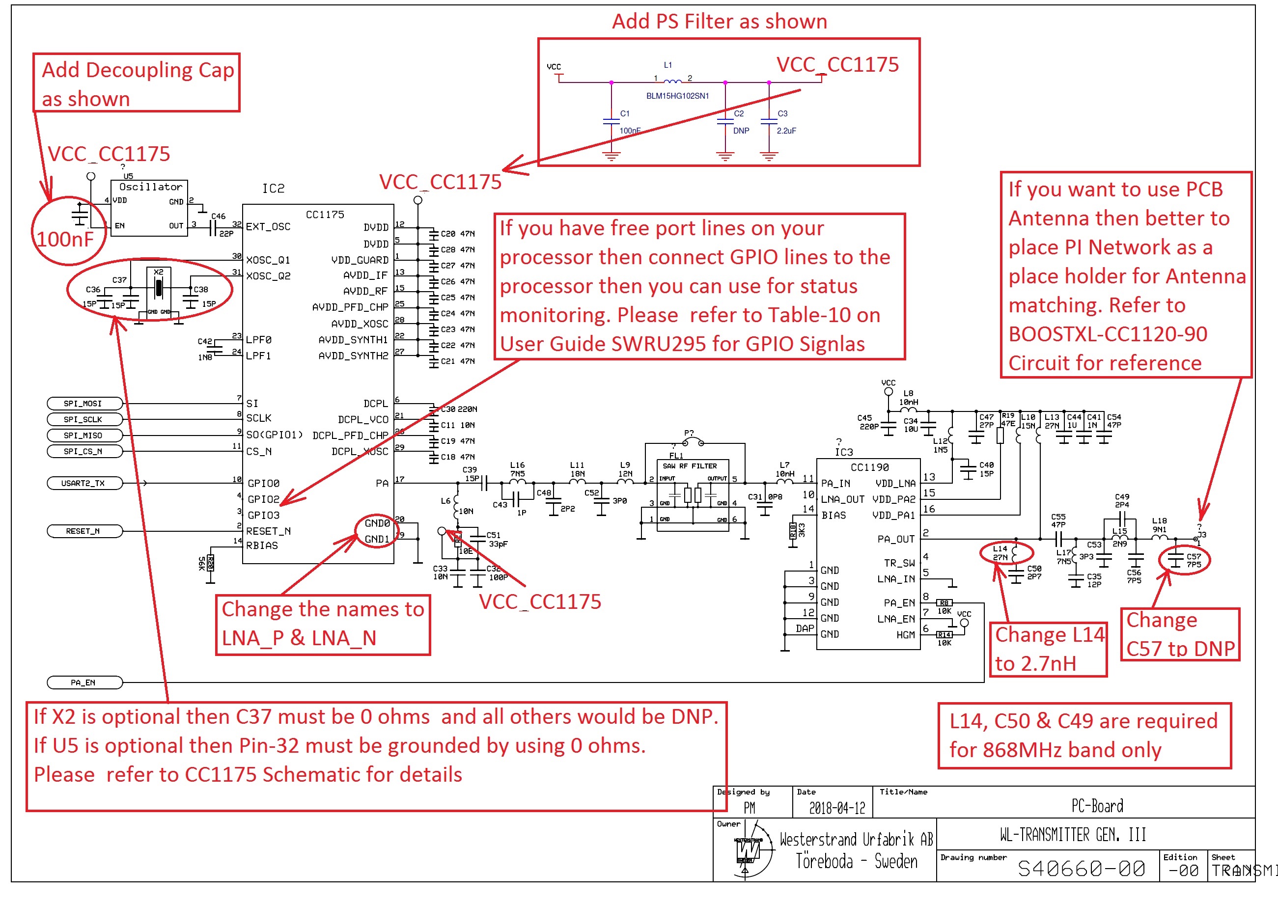
I'm working on the design of a radio transmitter for 869.525 MHz 500mW. I use CC1175 and intend to connect the CC1190 to have more power. I've got it working with the development system using the CC1175 only . Now I'm adding the radio components to my own circuit board and intend to connect the CC1175 and CC1190 together. When I look at the different reference designs, there seems to be a lot of components used for radio reception. Since the CC1175 is just a transmitter circuit and I need the solution as small as possible, I want to remove everything that is not needed. Can someone help me just to delete the unnecessary components on the design drawings?

I use the reference designs CC1175EM_868_915_schematic.pdf and BOOSTXL-CC1120-90-Sch-A.pdf

Regards,
Per Magnusson

  • Hi,

    If it is for Tx Only , then you can remove everything in between C174 and P3 (Keep C174 and remove C3) and the circuit (Blaun) on Pins 19 & 20 of CC1175 except C201 (0 Ohms) and L192 (0 ohms) on CC1175EM Schematic .
    Connect C174 output to the input of (Pin-5 - CC112x_RF) ON BOOSTXL-CC1120-90 Schematic Page-2. You need everything on Page-2 of the Schematic except P6.

    You can post your Schematic in PDF, when it is ready. We can review it.

    Thanks,
    PM
  • Thank you for the answer.
    Can I also remove the SAW filter (FL2) on the  BOOSTXL-CC1120-90 schematic diagram? Any other components that can be removed on the  BOOSTXL-CC1120-90 page 2 schematic?

    Regards,

    Per

  • Hi,

    We are discussing internally on this topic and I will get back to you soon with proper solution.

    Thanks,
    PM
  • When the CC1120+CC1190 reference design was made the SAW filter was required on the highest power levels since the phase noise made the board fail the limit around 863 MHz without. The restricted band edge has been changed in the last EN300 220 to be at a lower frequency meaning that it's possible that the design will pass without SAW filer but I don't have any boards without SAW filter to test with. To be on the safe side you can include a SAW filter but also a 0603 footprint under the SAW filter to bypass it to simplify testing if wanted.
  • Hi,

    We discussed internally and we recommend the following.

    CC1175 Schematic:

    • Remove L191, C201, L201, C191, L192 & L193
    • Ground Pin 19 (LNA_P) and Pin 20 (LNA_N) on CC1175
    • Remove the connection from Pin-18 ( TRx)  to C181
    • Ground C181
    • Remove P3 and connect this port to the SAW Filter

    CC1190 Schematic (BOOSTXL-CC1120-90):

    • Put an option (0603 Foot print ) to by-pass, if SAW Filter is not required ( as suggested by TER)
    • Remove C34 and Ground Pin-5 (LNA_IN)
    • Remove the connection from Pin-4 ( TR_SW)  to C36 and Ground C36
    • Replace J3 with 0 Ohm Resistor ( this will be helpful for testing. if you want you can keep the connector)
    • Remove P6
    • Connect R23 to VDD_CC1190
    • Remove R24 and Ground Pin-7 (LNA_EN)
    • Connect R25 to VDD_CC1190

    Please post your Schematic in PDF for our review, when it is ready.

    Thanks,

    PM

  • Thank you for your help. I will implement this in my schematic and post it for review when I am ready.

    Regards,

    Per

  • Hi PM
    In earlier post you said "Connect C174 output to the input of (Pin-5 - CC112x_RF) ON BOOSTXL-CC1120-90 Schematic". Meaning that I shall remove L172, C176, L173, C175, C177, L174 and P3. Is this still the case considering previous post?
  • Hi,

    No, those are required. So, please keep them.

    The following is our consolidated final list. Please follow this and ignore all the other previous posts.

    CC1175 Schematic:

    • Remove L191, C201, L201, C191, L192 & L193
    • Ground Pin 19 (LNA_P) and Pin 20 (LNA_N) on CC1175
    • Remove the connection from Pin-18 ( TRx)  to C181
    • Ground C181
    • Remove P3 and connect this port to the SAW Filter

    CC1190 Schematic (BOOSTXL-CC1120-90):

    • Put an option (0603 Foot print ) to by-pass, if SAW Filter is not required ( as suggested by TER)
    • Remove C34 and Ground Pin-5 (LNA_IN)
    • Remove the connection from Pin-4 ( TR_SW)  to C36 and Ground C36
    • Replace J3 with 0 Ohm Resistor ( this will be helpful for testing. if you want you can keep the connector)
    • Remove P6
    • Connect R23 to VDD_CC1190
    • Remove R24 and Ground Pin-7 (LNA_EN)
    • Connect R25 to VDD_CC1190

    Please post your Schematic in PDF for our review, when it is ready.

    Thanks,

    PM

  • Hi, Here is my schematic diagram, please review.

    Thanks,
    Per

    S4066000.pdf

  • Hi Per,

    Attached is the Review.

    If you need any clarification, please let me know.

    Thanks,

    PM

  • Thank you for your help, it is much appreciated.
    Just one comment: LNA_& LNA_N does not exist on CC1175, pin 19 and 20 is GND (0V)

    Regards,

    Per

  • Hi,

    Yes, I agree with you. But in our CC1175 Reference Design, it shows LNA_P & LNA_N. That's why I made the comment. I think that applies to CC112x device.

    Thanks,
    PM
  • Hi,

    I have an additional question regarding the BOOSTXL-CC1120--90 schematic diagram. I can see that a dual matching filter from Murata (LFD21868MMF1D386) is used between CC11XX and CC1190. Can this type of filter also be used on the output of CC1190 this to reduce the number of discrete components?

    Regards,
    Per

  • No,
    since CC1190 require different impedance compared to CC1120.
  • Ok, thank you.