Other Parts Discussed in Thread: CC2650
All,
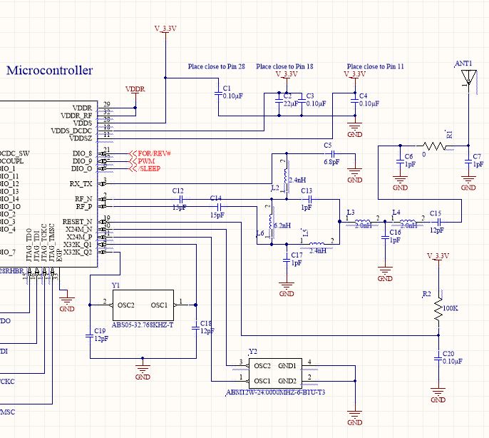
I am working on a design utilizing a CC1350F128RHBR with BLE only wireless communication. I have followed several TI App notes and reference designs are would like to share the RF side of my design in the hopes that the community would have some feedback.
I am modeling this question off this post.
My use of the CC1350 is intended to be BLE only at this time. A future spin of the project may make the jump to Sub 1GHz and thus the SW folks wanted to start with the CC1350 instead of the CC2650.
The overall board size is 16.5mm X 58mm. The desired BLE range for this initial board spin is <10' . The board will be packaged inside an electrically floating metal housing (not my idea) and communicating with a tablet sitting next to the case. Brief testing of a cheap BLE fitness tracker placed in the housing shows communication to the tablet. Off of that (admittedly limited) basis, we jumped into the design.
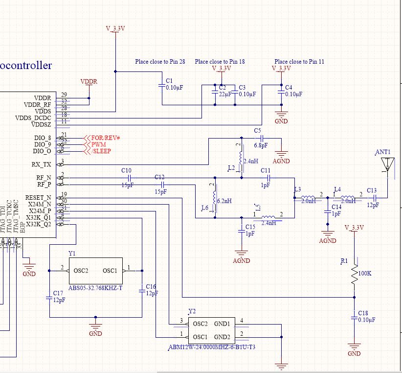
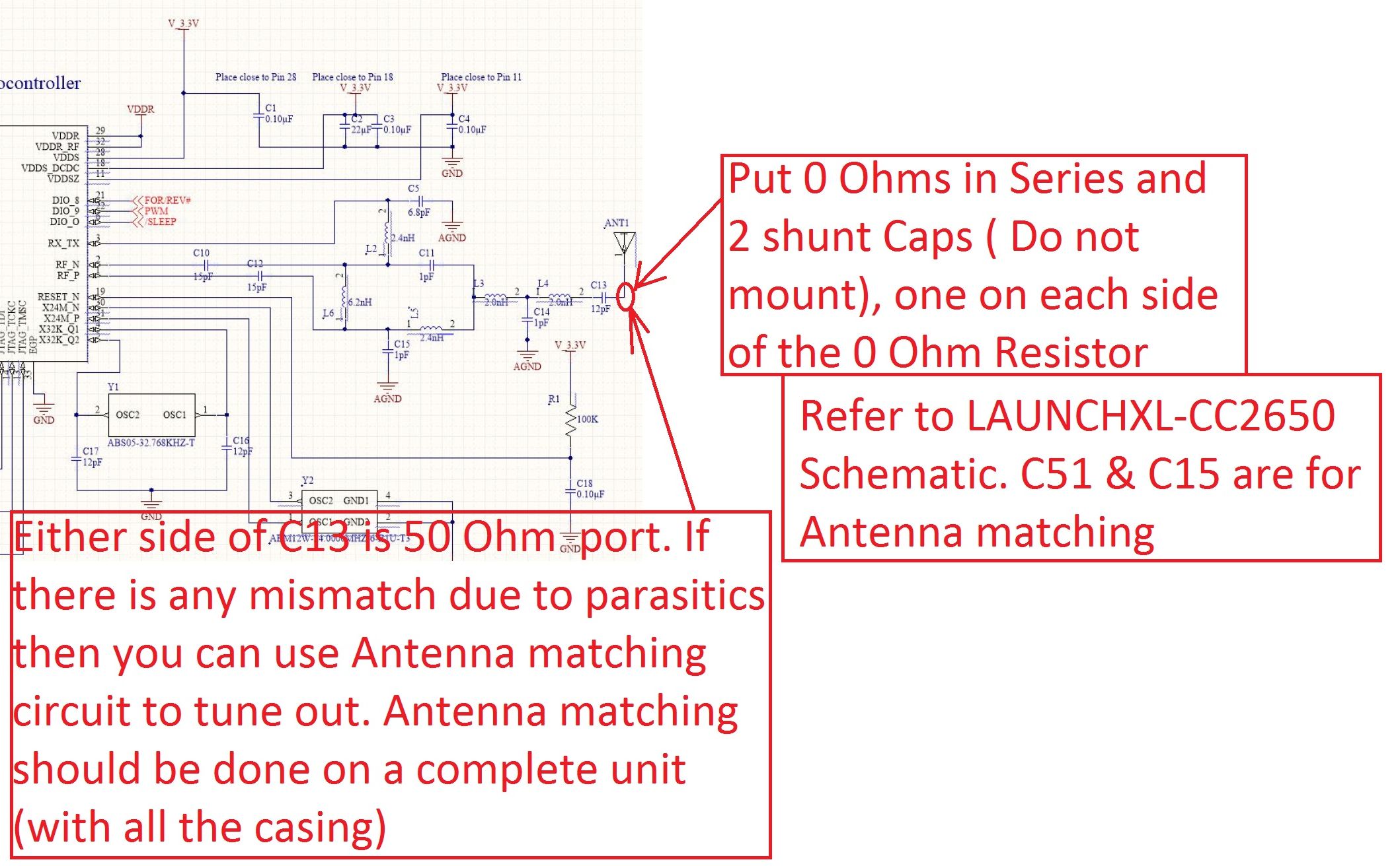
For my schematic design, I referenced the CC2650 Datasheet (specifically Figure 7-1, shown below). My schematic implements differential operation.
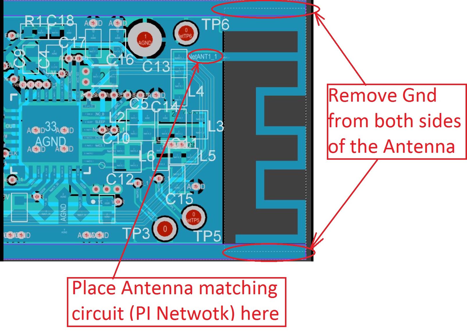
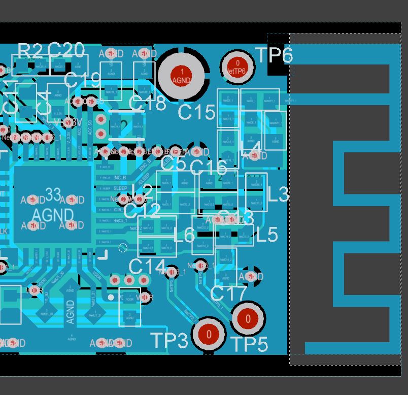
My antenna design is copied from AN043, Small Size 2.4 GHz PCB antenna (swra117d.pdf). I copied the Inverted F Antenna from the files provided by TI and imported it into my design. The antenna fits perfectly into the space I have available on my board and thus I have not modified the layout or dimensions it in any way.
I am using the Solidworks PCB package. I am usually a Cadence guy but my new gig uses Solidworks PCB. It drives like Altium in most ways but not all.
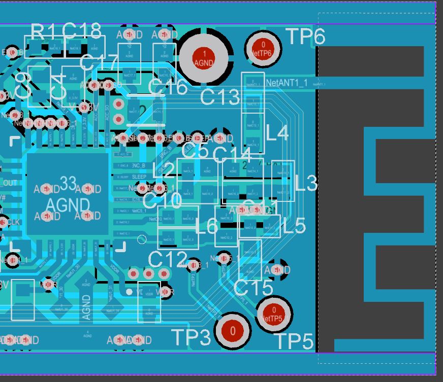
My board is 6 layers, SIG/GND/SIG/CORE/PWR/GND/SIG. 0.031" thick. 1oz copper. Top and bottom of the board are flooded and tied to GND.
Impedance calculations for the NetANT1_1 trace between C13 and the feed point come back as 83.8Ω. That seems a little high to me but to get it down required a flood between C13 and the antenna and that is not what I am seeing in reference designs.
Questions:
In my schematic I have most things tied to GND and the antenna connections to AGND. In the layout these are implemented as the same net. Does anyone see value in keeping them separate and tying them together at one point? I know this depends a lot on the reset of the design but I am less sure what to do related to the RF part.
Has anyone laid out a Differential Operation Antenna as shown in the CC2650 datasheet and then later DNP and 0Ω components to change to Single Ended Operation? I started with differential for the better performance but may want to cost and size reduce to single ended if possible. It seems like I could pop some parts off a board and 0Ω some others and have a crude conversion. Just wondering if anyone has tried this and can share what they found.
Am I missing anything glaring? I have a few ARM core micro designs under my belt but this is my first RF design and the first project where I was the sole person working on the layout.
Any help is greatly appreciated.