This thread has been locked.

If you have a related question, please click the "Ask a related question" button in the top right corner. The newly created question will be automatically linked to this question.

CC2430DB_REFDES: Impact of copper thickness for the antenna ?

Part Number: CC2430DB_REFDES

Hi,

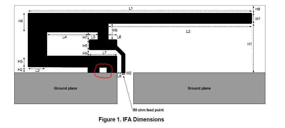
I would like to know if the reference design for CC2430DB wherein it shows the dimensions of 2.4Ghz antenna is affected by the thickness of the top layer copper plane.

Whats Cu thickness was the design made for? and how will the dimension change for a 1 oz and 2 oz copper top layer option?

Thanks.

  • If you are looking for an antenna I would advise to look in www.ti.com/.../CC-ANTENNA-DK2. The layout files contains the stack-up of the PCB, including copper thickness.

    I don't think the copper thickness will impact the antenna too much. It's not possible for me to double check at the moment since the expert is on vacation.

    Why do you want to use a thicker copper layer than used in our ref designs?
  • We have a 2oz top layer board to ensure we minimize trace resistance since we have high current circuit on that layer as well for other purposes.

    It be nice if you can ask when the engineer returns from vacation if the thickness matters or not for certain.

    Thanks.

    Regards

    Samuel. C

  • Found this: 

    Radiation resistance is that part of an antenna's feedpoint resistance that is caused by the radiation of electromagnetic waves from the antenna, as opposed to loss resistance (also called ohmic resistance) which generally causes the antenna to heat up. The total of radiation resistance and loss resistance is the electrical resistance of the antenna.

    The radiation resistance is determined by the geometry of the antenna, where loss resistance is primarily determined by the materials of which it is made. While the energy lost by ohmic resistance is converted to heat, the energy lost by radiation resistance is converted to electromagnetic radiation

    Meaning the copper thickness impacts the efficiency. 

  • Hi,

    1) Could you confirm your answer with the Expert Engineer who was on vacation few weeks ago. It is better to understand and be sure.

    2) Also I have highlighted by circling in red color the aspect of the antenna which has a small rectangle of no copper area, There are no dimensions given for that cutout area and your document DN0007. May I know to understand why it was so and it's significance?

    Thanks.

  • Hi,

    The CC-Antenna-DK2 is designed with a top layer metal thickness of 35 um (1 oz copper). If the copper thickness is increased then the loss resistance will theoretically decrease. The delta between the 1 oz and 2 oz will be very little in terms of loss resistance since the power is very low.

    The radiation resistance is dominated by the feed point position of the antenna and this will not be effected by the increase in copper thickness.

    The performance of this antenna with 1 oz of copper is very good and I would not use extra copper thickness . The benefits will not be noticed and the PCB will be more expensive.

    For the dimensions shown in the red circle, please refer to the gerbers. This was originally designed to allow for increased bandwidth (and slight tuning) since this effectively increased the distance of H1 to the GND layer.

    Regards, Richard