This thread has been locked.

If you have a related question, please click the "Ask a related question" button in the top right corner. The newly created question will be automatically linked to this question.

CC1310: RF Trace Impedance Values?

Part Number: CC1310

Hi,

I've laid out plenty of single end 50 ohm traces for RF systems.I can calculate the impedance of my traces based on my board stack-up.

I have not laid out a system with these multiple lines that get impedance transformed in the balun.

(I'm basing this question on the LAUNCHCL-CC1310 REV 1.3.0 schematic component names).

What is the strategy here for runing the RF_P, RF_N, and RF-TX lines?

What impedance of the traces as they run from the IC and go through L22, L23, C21, C22, L12, and C11?

After that transformation, what should the trace impedance be through C12, L13, C13, L14, C14, and C15?

I'm guessing after the two network, ostensibly the signal is now 50ohms?

(I'm going to put one PI network in front of our final antenna for VNA testing on prototype boards for final tuning).

---

On the LaunchXXL-CC1310 layout, I see the traces begin at ~0.31mm, and then change to ~0.41mm after the balun. What is going on there just in terms of the impedance transformation?  

What impedance is the 0.31mm section?  What impedance is the 0.41mm traces suppose to be?  (I can adjust our trace width to match the impedance, etc.).

Thanks,

  • The only 50 ohm point in this design is before the pi network for antenna tuning.

    Note that the line used here is very short and can therefore not be regarded as transmission lines with a given impedance.

    When using 0402 components the footprint is of a size that makes it natural to route with a trace that is between 0.3 and 0.4 mm thick. You will not see any performance change if you select on or the other.
  • @TER -- thanks, I'm looking at the SWRC316, the SimpleLink CC1310 4-Layer 4x4 Differential 779-930 MHz v1.0.0 Design Files.

    Have you guys measured improved TX transmit strength using a differential layout vs. the single ended CC1310 Launchpad layout?

    I've got space to layout a nice clean differential path. If we can eek out anything extra doing the differential layout, it's pretty much free from our perspective.

    Typically I've always just used 50 ohm traces on a 4 layer board. What I know is magical about 0.3mm traces on a 4 layer board that they are pretty much 50 ohm traces (I think on our 4 layer board stack up - 0.314mm is 50 ohm). So when I see 0.3mm traces, I wonder if there is some layout issues

  • Not sure if I follow, what did you have in mind when you say differential layout?
  • Check:  , the top layer gerber.

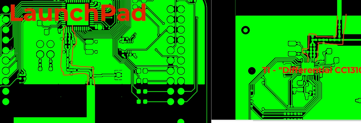
    They call this the "differential layout" -- "SimpleLink CC1310 4-Layer 4x4 Differential 779-930 MHz v1.0.0 Design Files" vs. the Launchpad gerbers.

    (I see both traces are about 0.3mm...).

    I've got a screenshot of both.  You see how in the differential layout it's got that symetry, but in your Launchpad it isn't .

  • Check: www.ti.com/.../swrc316, the top layer gerber.

    They call this the "differential layout" -- "SimpleLink CC1310 4-Layer 4x4 Differential 779-930 MHz v1.0.0 Design Files" vs. the Launchpad gerbers.

    (I see both traces are about 0.3mm...).

    I've got a screenshot of both. You see how in the differential layout it's got that symetry, but in your Launchpad it isn't .
  • The antenna is single ended, how do you plan to do this?
  • Yeah, so why does TI call this the "differential" layout then? (I've only ever done single ended output, not a transceiver)? I'm asking to learn, not be combative. ;)

    I was just going to use passives as in the reference design, and I was planning on adding one additional PI network to fine tune the antenna with a VNA.

    The signal is going to run to a 50 ohm metal helical.

  • I want to point you to this:

    ww1.microchip.com/.../Atmel-42131-RF-Layout-with-Microstrip_Application-Note_AT02865.pdf

    ---

    Section 3, 100Ω Balanced Microstrip . I was kind of thinking this is what the CC1310 has going on. We would want two 100Ω lines, and then they transform into one 50Ω line through the balun network as per the Atmel write-up.

    I pinged TA to weigh in here.  Is he around?  I know he said he'd clear this up if/when we ever got the frequency hopping working as we needed.

  • I think I may have misunderstood you: "You see how in the differential layout it's got that symetry, but in your Launchpad it isn't ." For me the layouts looks quite similar, the only difference I can see is that the filter part is done slightly differently to fit with the size of the board. Which symmetry exactly do you mean is lost?
  • On the differential example, you can see that the traces are mirror opposities. Where with the Launchpad the traces are not mirrors. Very close though.

    I think really why I am pushing, it was just that TI calls this out as something specific.

    What about the trace impedances though as called out by that Atmel note? Can you get a specific answer if that is how we should layout the RF traces for the CC1310? I have no idea the output impedance out of the IC, and anything that is going on in the balun and moving forward.
  • I may be double-posting.

    The forum is acting weird on my browser. On the differential layout, it appears that the traces are a mirror image which equal spacing like they are differential lines.

    TI seperately calls out that design, so I'm wondering.

    More directly though, should we be treating those lines as 100 ohms unbalanced, and then after the balun as a 50 ohm balanced line feeding to the antenna (as per the Atmel note?).
  • In the ideal world the RF_P and RF_N traces should have been a perfect missor image of each other. But I doubt that you will see any real difference if you had simulated the two designs in ADS or similar and compared the s-parameters.

    If the RF_P and RF_N traces have different length causing a phase shift of several degrees the performance will degrade but with the difference here you will not see any difference.
  • I'm coming to Dallas if this RF layout is whack! ;) -- I followed the layout pretty faithfully.  If I do say, it's pretty symmetrical.  Man do I wish that crystal was not close to those pins...  tight fit for a design that has existing mechanicals.

  • I'm not located in Dallas so I still feel safe ;)

    In a RF design filter every other cap to ground should be rotated 180 degrees. This is to avoid the RF signal going from one ground pad to the next without getting filtered.
  • No kidding, I have never heard that before on the RF filter layout!  See you learn something new everyday, I'll flip this around.  (Yikes, that means I have a design with 50k+ units out there that should be flipped!).

  • If you have plenty of vias to ground and a solid ground plane you should see limited difference between flipping every second cap or not but this if RF and RF signals takes a shortcut when it's possible so better safe than sorry.