This thread has been locked.

If you have a related question, please click the "Ask a related question" button in the top right corner. The newly created question will be automatically linked to this question.

CC1110EM868-915-RD: DN023 antenna design problem

Part Number: CC1110EM868-915-RD

Hi,

I've designed my new PCB using the DN023 as a reference for the 915MHz PCB antenna.

The dimensions of the antenna are exactly the same. My ground plane is slightly bigger (35mmx46mm instead of 31x45). The PCB thickness is 0.8 mm as advised.

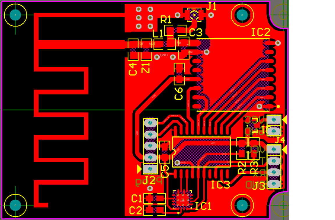
As "no external matching components are needed", only L1 is populated with a 0 ohm resistor.

J1 is used as an external ufl connector for tests purpose (when R1 is populated with a 0 ohm resistor).

Since the last part of the antenna is here 3mm long, it should be calibrated for 900-915MHz. But my tests show very different results.

When I've tested my design, using 1/4 wave length (82mm) wires as antenna give a way better signal strength than using that PCB antenna.

Here are some measures of the VSWR / return loss of the antenna :

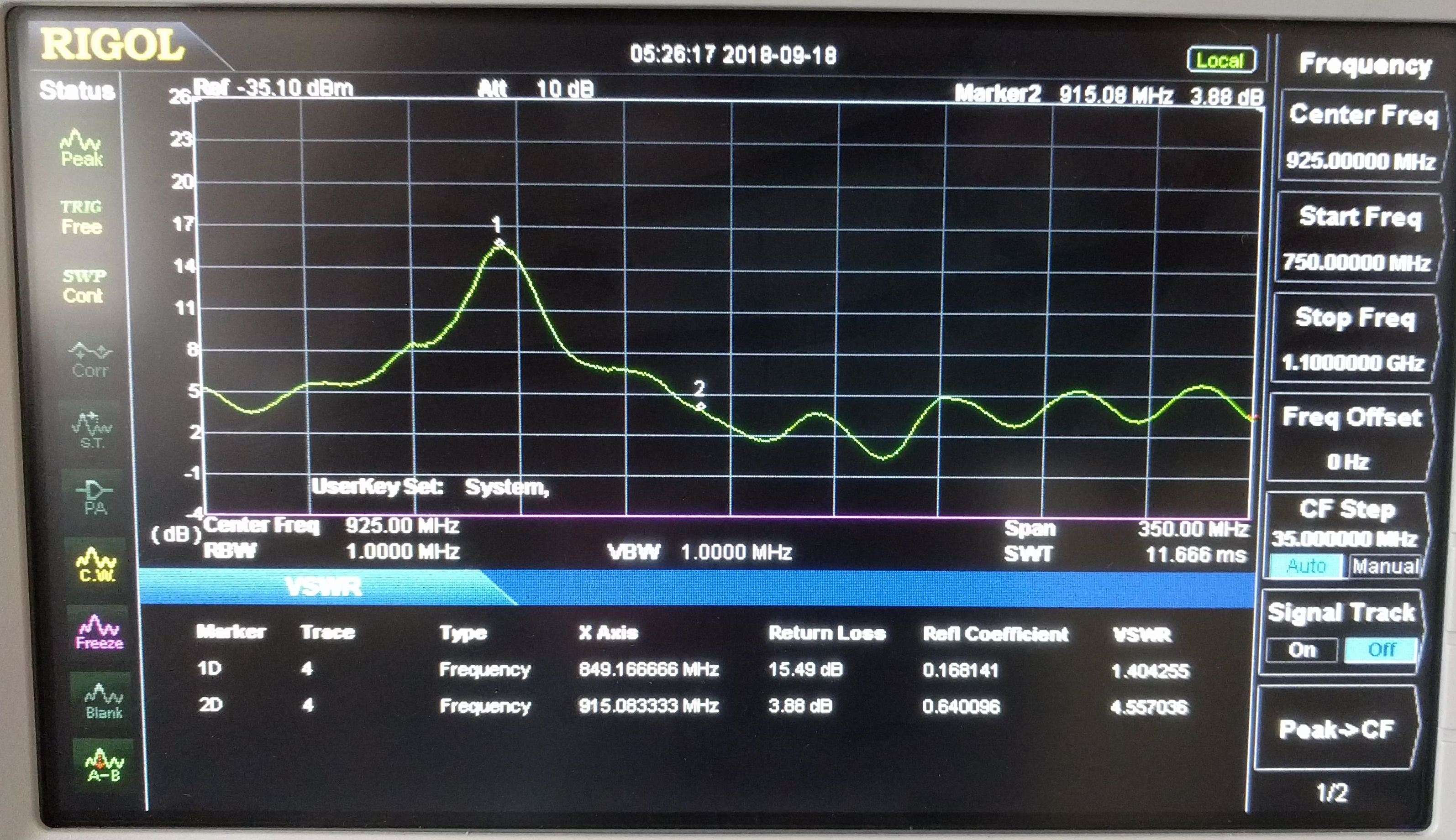
The VSWR is best at 850MHz.

After cutting a few millimeters of the antenna length, the frequency increase, but it doesn't match the Design Note.

To prove that the measures are accurate, I've also tested a reference antenna.

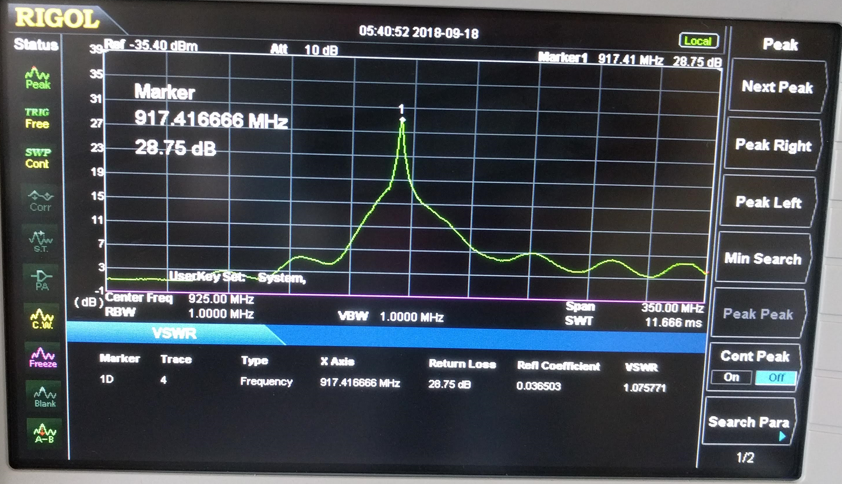
That is a perfect result.

What could be wrong in my implementation of this design?

Do you have any suggestion for it to work?

  • Hi,

    TI always recommends to include a pi-filter for antenna matching even if the measurements indicate that a match is not required. The resonance of the antenna is easily affected by surroundings, casing or nearby objects. With an antenna match network, the mismatch can be compensated for and a new revision of the PCB will be avoided.

    The antenna consists of two elements: first is the actual antenna element and the second is the size of the GND plane. By changing the GND plane size from the reference design will also introduce a delta in the resonance. If your GND plane is larger then the reference design, then this should cause the resonance to move downwards so the antenna length can be too long.

    Regards,
    Richard
  • You have introduced a stub (the trace that goes to R1). This can introduce mismatch. You could place the R1 pad over the L1 pad - this way there will be no stub - and you will of course only place one of the components...
  • Hi,

    The pi-network is created by C3, C4 and L1. I may be able to use components with a smaller footprint, 0603 instead of 0805, to reduce a possible inductance. Adding the matching components is definitely the way forward, I'll get a Vector Network Analyzer. That's the only way, as I realize, to understand the antenna and choose the perfect match.

    I didn't imagine that such a small change in the ground plane would modify the frequency so much. But it makes sense. The area of my ground plane is about 15% bigger than the reference design, and the target frequency has decreased by 5%.

    Thank you for these tips.

  • The next revision will include that modification.
    Good advice, thank you.