This thread has been locked.

If you have a related question, please click the "Ask a related question" button in the top right corner. The newly created question will be automatically linked to this question.

CC1352P: Additional preliminary information

Part Number: CC1352P

Hi team,

My customer needs to know additional preliminary information that not yet listed in the datasheet to calculate average current consumption and link budget.

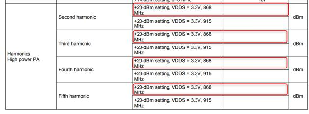
  1. Do you have any test results of output power when voltage is 3.0?
  2. Do you have a preliminary data to share for this fields?

  3. Can we proof the customer that CC1352P will not be damaged when transmitting +20dB with some components in RF path unsoldered due to manufacturing issues? It’s very important for them.
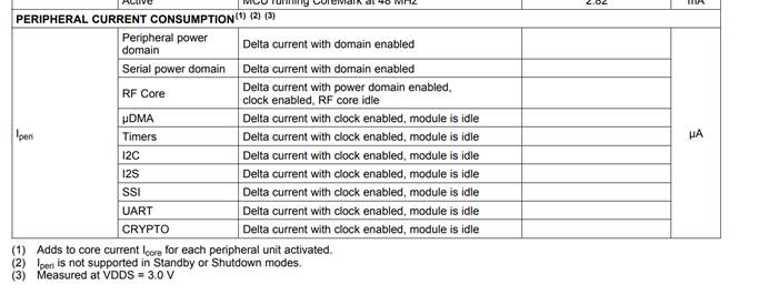
  4. There is no description of how much GPIOs are consumed in sleep mode if they are active(high or low with unloaded outputs). We are talking about the fact that we put on the output state and go to sleep.
  5. Please provide the impedance values on all RF outputs of the chip.

Best regards, Vsevolod.

  • Hi Vsevolod,

    Characterization is ongoing and we will updated the datasheets before RTM. As of now, there is no more preliminary data to share. Outout power for the PA at 3.0 V will be close to 20 dBm. The reference design boards will be designed such that the harmonic levels are within typical regulatory requirements.

    The 20 dBm PA will handle transmitting at full power without any matching components.

    The GPIOs themselves do not consume any power when they are unloaded.

    We do not provide impedance values for the RF ports as described here: processors.wiki.ti.com/.../CC26xx_Optimal_Load_Impedance . The customer should follow the reference designs closely to achieve the expected RF performance.

    Best regards,
    Fredrik