This thread has been locked.

If you have a related question, please click the "Ask a related question" button in the top right corner. The newly created question will be automatically linked to this question.

CC1310: cc1310

Part Number: CC1310

We are going to develop Grade 3 security system based on CC13X0 TI chipset. This standard required to support dual band frequency communication in order to meet “EMI Interference spec”.

For this approach we are planning to implement dual Sub 1GHz 433/868 MHz band for Europe market.


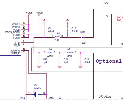
According to TI CC1310 reference design with single ended application, it seems  we can use 2 different bands TX/RX from each ports for example 433MHz from Pin1 and 868MHz from Pin 2.

Do you think it will work properly?

What will be performance?

    1. TX Output power at each Pin 1,2?

    1. Rx sensitivity at each pin 1,2 ?
    1. Could we meet FCC and EN spec ? what about 2nd harmonic (single end use)?


Please advise,

  • Having separate paths for 868/915 MHz and  433 MHz is just fine.

    Generally: The output power for a single-ended design will be 3 dB lower than a differential design (voltage swing is half). The sensitivity for a single-ended design will be approx. 1 dB lower than a differential design.  A single-ended design will meet both FCC and ETSI  regulatory requirements.

    The sub-1 GHz part from can be used for a single-ended 868/915 MHz design. Note that the antenna matching components are different for US vs Europe. Reason being that the PCB antenna has a finite BW  and is not wide enough to cover both frequency bands without tuning the antenna match.

    We have not done a 433 MHz single-ended design. As a starting point the bottom network in the picture below can be used. This has not been thoroughly tested. Between the C16 and the antenna you should add a series capacitor (dc block) and then the antenna impedance matching components.