Other Parts Discussed in Thread: CC1312R
Hello,
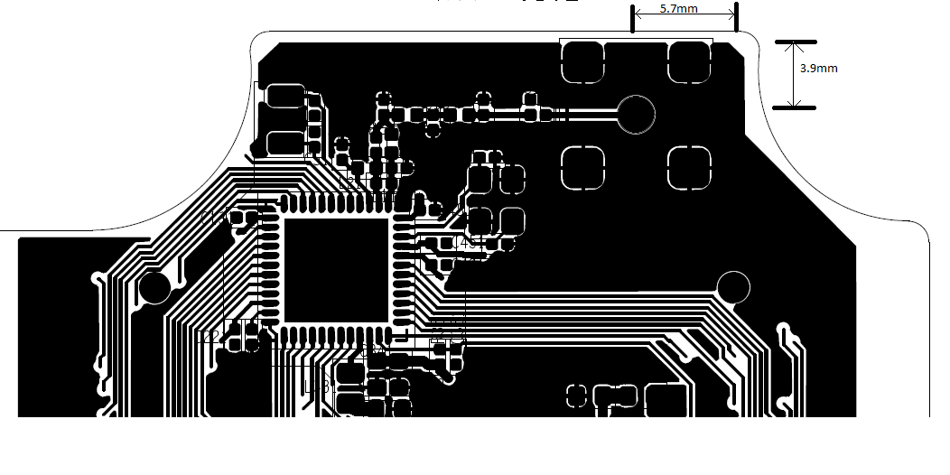
we are designing our new pcb of cc1310.
here i attached gerber file for the new design.
kindly review it, let us know if any error.gERBER FILES.zip
Hello,
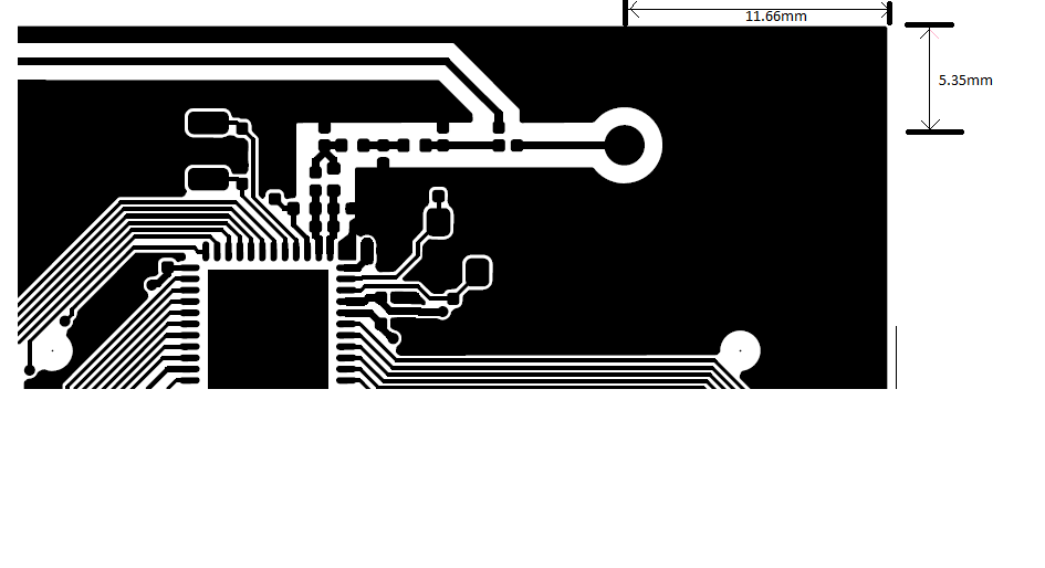
we are designing our new pcb of cc1310.
here i attached gerber file for the new design.
kindly review it, let us know if any error.gERBER FILES.zip