This thread has been locked.

If you have a related question, please click the "Ask a related question" button in the top right corner. The newly created question will be automatically linked to this question.

CC1310: uLDO fails when system goes into standby mode

Part Number: CC1310
Other Parts Discussed in Thread: TPS54240, BQ27441-G1, BQ24074, TPS63051, TPS63020, TPS61099, LP55231, TPL5010, TEST2

We have a rare issue where our cc1310 does not recover after going into standby mode. However the issue does not appear on CC1310 revision A.

We narrowed this problem to uLDO.

Setup:
cc1310 is used in combination with many devices:
- Power path
    - step down DCDC converter regulating to 5V (tps54240)
    - powerpath management IC with charger(bq24074); fuel gauge(bq27441-g1); 3.7 Li-Ion, 2 cell battery pack
    - buck/boost IC regulating to 3.3V (TPS63051), buck/boost IC regulating to 3.8V(tps63020)
    - boost converter regulating to 3.3V(tps61099)
- Peripherals:
    - Devices connected through i2c bus:
        - Quectel L96
        - bq27441
        - LP55231
        - mcp9804
        - BMI160
    - Devices connected through second bus:
        - Telit LE910 modem
    - Devices connected through SPI bus:
        - W25Q32 (flash memory)
    - external watchdog (TPL5010)

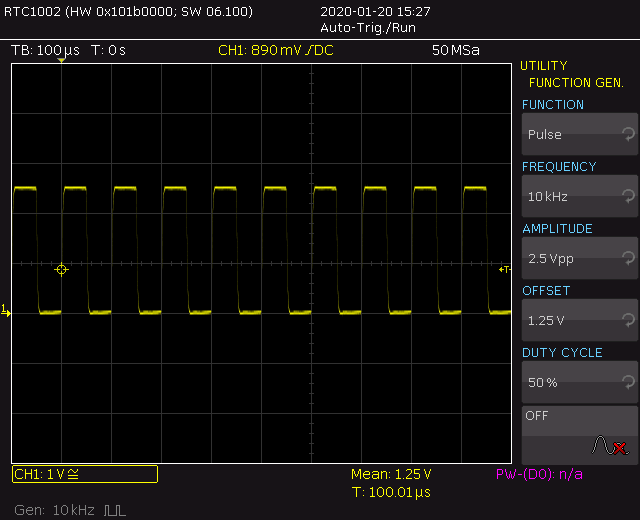
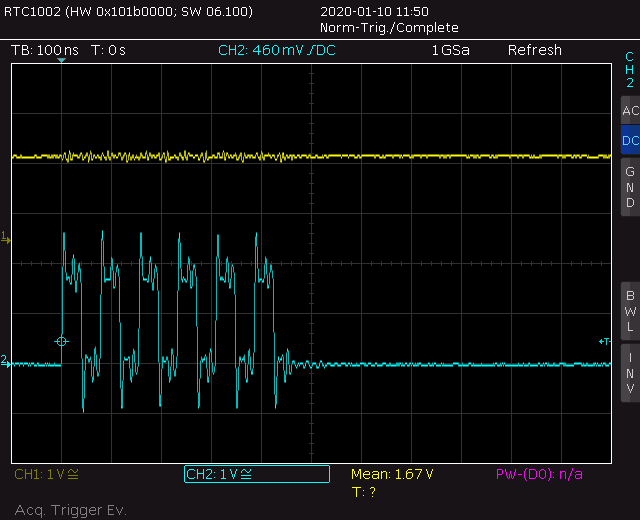
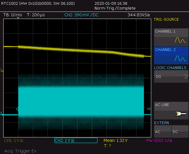
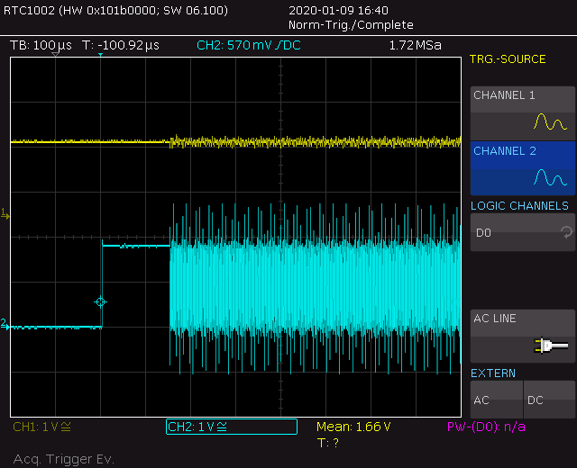
We noticed that when cc1310 is put to standby mode and right after a signal is sent on DIO14 ( signal is square wave, 2.5Vpp 10kHz) voltage on DCDC_SW will drop to 0V and 32kHz xtal will shutdown. to get out of this state cc1310 has to be reseted (done by external watchdog).
If we configure to use digital LDO device is working correctly and never fails. DIO14 is configured as input, pull down. If pin is configured as output system will not fail.

This issue is very severe as we have some units where uLDO is permanently damaged. 


Also, when uLDO fails TPL5010 will trigger after double the set time. we verified that it is working properly in other cases. 
  • I forgot to mention that we have managed to replicate this behaviour on a LaunchPad with only our SW and no extra devices connected. 

  • Kostianty,

    We will look into it and get back to you ASAP. Please bear with us.

    BR,

    Seong

  • Could you provide a plot showing the signal you are applying on D14? 

  • Here's the signal we use. 

    Here's the signal that triggered this path of investigation. 

  • Could you give more details on the difference between the first and second plot? 

    Is what is shown on CH1 in the first plot or is it the signal that is shown on CH2 on the second plot that is measured at DIO14?

  • On the first plot is the signal from the generator, measured on DIO14. 

    On second plot CH2 shows real world signal, that we've noticed in our device, measured on the DIO14. this signal is produced by IO pin of another device and should not be there during deep sleep state. But it might happen from time to time and should not influence the operation.

  • The signal you show on CH2 goes down to - 1 V which is outside the absolute ratings of the chip. Hence it's of significance if the issue you see is only with CH2 signal or both.

    You wrote that you are able to recreate the issue on a LP. Does this happen if you apply this signal to any DIO or just DIO14? 

  • I was very careful to reproduce this issue with pure square wave that was from 0 V. 
    I've tested on several DIOs, but DIO14 is the only one that is not used in our FW. We could try to setup another pin in the same way and re–test.

  • We re–tested with cc1310 rev A with the same exact configuration and it would never fail. 
    Is it possible that we are on some edgecase? I would expect all cc1310s fail with this setup, but only Rev B fails. 

    Also, empty cc1310 would not fail, not sleeping unit will not fail and using Digital LDO will not fail. Only unic configuration with uLDO and deep sleep will fail.

  • It would be very useful if you could provide an example we could run on the Launchpad and see the issue. 

    I'm not aware of any difference between rev A and B that could explain this.

  • Sure, can I send you binary in private? 

  • Yes, I accepted the friend request. But I would like the source code to be able to see what is going on. 

  • Does that mean you are unable to trig this using TI-RTOS, only with your Contiki version? 

  • We never tested with TI-RTOS as we never used it. 

    One thing that we can't get a grip of – why does it happen only with uLDO and not digital LDO. 

    An extra question – assuming we had that signal with -1V spike for some time, would it be possible for uLDO get damaged permanently? And why would signal on IO pin have any influence on uLDO in the first place.

  • I don't think the issue is related to the uLDO. I suspect that for what ever reason the 32 kHz xtal stops. Then VDDR will either go to VDDS (which will be fatal) or to ground. 

    Are you using Contiki NG and the version that is based on our drivers or a different version? I'm not familiar with contiki hence I'm curious if you manage to trig this with one of the examples in the CC1310 SDK. I want to see if this also is tied to software somehow or if it's just a hardware usage issue. 

    Would you be able to do a test where you are not using the 32 kHz xosc but using the 32 kHz RCOSC? If this works this is related to the xtal. 

    If a signal goes to -1 V on a DIO means that the ESD protection is conducting and charge will be pumped into the substrate of the chip which could change the transistor behavior. The 32 kHz xosc runs on very low power and in effect changing the transistor parameters could be enough to affect the driving strength of the module. 

  • Hi TER,

    I work with Kostiantyn, but on the software-side.

    > Are you using Contiki NG and the version that is based on our drivers or a different version? 

    We are still on Contiki, using cc13xxware v2.04.03.17272 - however the deep-sleep (lpm.c/.h) should be identical to NG (and as far as I can tell it follows the example in the cc13xx TRM).

    > Would you be able to do a test where you are not using the 32 kHz xosc but using the 32 kHz RCOSC?

    We can but it might take me some time to familiarize with those parts to get it right.

    Regarding the binary sent to you I believe the key parts are:

    1. DIO 14 being set to input and pulled low

    2. Node going into standby mode for 30 sec, wakeup shortly, then standby mode again.

    (3. Send signal on DIO14 and observe failure)

    Do you perhaps have a TI-RTOS example which easily could be modified to match this? (I do not believe the duration of the standby mode is critical as long as it is not very short)

  • I believe the "empty" example could be used. 

    For using the RCOSC instead, see CCFG.c or similar (not sure what's used in contiki)

  • I have a small update on the issue. 

    I made a mistake on the generator – it was on the wrong offset and most likely negative part of the pulse was triggering the issue. But just to be sure I've re–tested. So without zero crossing all is working ok. with pulses going from -1.25 to 1.25 V, turned on when device going to sleep. But if I keep signal on all the time and after that device is going to sleep – all is ok. Same thing for the digital LDO – it will not trigger any problems at any conditions.

    Also, we have several cc1310, that fail even without external source of noise, just with using uLDO during standby mode. I believe there's a permanent damage somewhere on the powerpath, but I am not sure where at this moment. Any guesses why it fails only with uLDO?

  • As I read your last post: In the first part you write that everything works independent of test method. In the second part you write that it fails regardless of test method?

    If I read correctly, why two totally different result for the same test? 

  • I had to re test all the states just to be sure what we see here.

    for all cases CC1310 going to deep sleep

    1. Power config for deep sleep: internal dcdc is used to power VDDR, uLDO is used in this mode. 

    - test1: square wave signal, 2.5Vpp with 0 offset(going from -1.25 to 1.25V) is applied to GPIO14 whyle MCU is in deep sleep. Result: DCDC_SW goes to 0, 32kHz crystal dies out. MCU needs external reset to run again.

    - test2: square wave signal, 2.5Vpp with 1.25V offset(going from 0 to 2.25V)  is applied to GPIO14 whyle MCU is in deep sleep. Result: all is working as expected, MCU comes out of deep sleep as expected.

    2. Power config for deep sleep: internal dcdc is used to power VDDR, Digital LDO is used in this mode. 

    - test1: square wave signal, 2.5Vpp with 0 offset(going from -1.25 to 1.25V) is applied to GPIO14 whyle MCU is in deep sleep. Result: all is working as expected, MCU comes out of deep sleep as expected.

    - test2: square wave signal, 2.5Vpp with 1.25V offset(going from 0 to 2.25V)  is applied to GPIO14 whyle MCU is in deep sleep. Result: all is working as expected, MCU comes out of deep sleep as expected.

    !Note: same test have been performed with Global LDO instead of internal dcdc regulator to the same results.

    These results have been replicated on custom HW and launchpad with the same SW(contiki OS with TI drivers)

    Next set of tests have been performed on a set of custom boards that we consider permanently damaged.

    1. Power config for deep sleep: internal dcdc is used to power VDDR, uLDO is used in this mode. 

    - test: run code from previous tests without any external signal applied to GPIO14. Result: DCDC_SW goes to 0, 32kHz crystal dies out. MCU needs external reset to run again.

    2. Power config for deep sleep: internal dcdc is used to power VDDR, Digital LDO is used in this mode. 

    - test: run code from previous tests without any external signal applied to GPIO14. Result: all is working as expected, MCU comes out of deep sleep as expected.

    An important observation that we've made on all the failing tests. On our custom boards we have a WD timer tpl5010. it is set to ~150s. When cc1310 fails this time is doubling. When we run successful configuration timer is working correctly. Same goes for not running any code on the MCU – WD is working fine.

  • Since it works with an input signal within the allowed limits, is it more for us to comment on? 

    For the second test, as I understand it the boards you have regarded as damaged have been subjected to voltages that are outside absolute maximum ratings for the chip which could have destroyed parts of the chip and hence I don't want to spend time on this since this is outside the datasheet. 

  • It's good to understand the source of the issue.

    Do you have any suggestion how we could mitigate it in the units that are in the field? Maybe some configuration of the pins that could protect the system?

  • I thought -2.5 V was a lab only issue. Is it possible to expose the pin with a voltage that is lower than 0 V in the field? 

  • Sadly – yes. We just found out that the modem we use has a weird power on behaviour where it bursts out relatively long pulse pack.

    This issue was never mentioned in the documentation and we haven't picked it up during testing for some reason. 

    On an important note – revA cc1310 units don't suffer from this issue at all, which is strange, only RevB cc1310.

  • I'm not going to look into why this is not an issue for rev A of CC1310 since the voltage you are applying is outside the levels stated in the datasheet. But it sounds like you have found out why the chip fails and that you in some way have to avoid the modem power on levels.