This thread has been locked.

If you have a related question, please click the "Ask a related question" button in the top right corner. The newly created question will be automatically linked to this question.

CC1352R: CC1352R + 0900PC15A0036 issue with poor RF output power

Part Number: CC1352R

We're having trouble with the output power of the 868MHz channel of CC1352R on our board (2-layer PCB).

Tried to run the same code on our PCB and LPSTK-CC1352R - LTSTK outputs 12 dBm when our gives only 6 dBm.

I've found one mistake in the copper - 0900PC15A0036 had a ground poly under its body. Tried to remove it (scratch from the PCB) - same 6 dBm.

Our RF engineer has a suggestion that 0900PC15A0036 can't operate properly on 2-layer PCB, but I didn't found any proofs in the documentation for that.

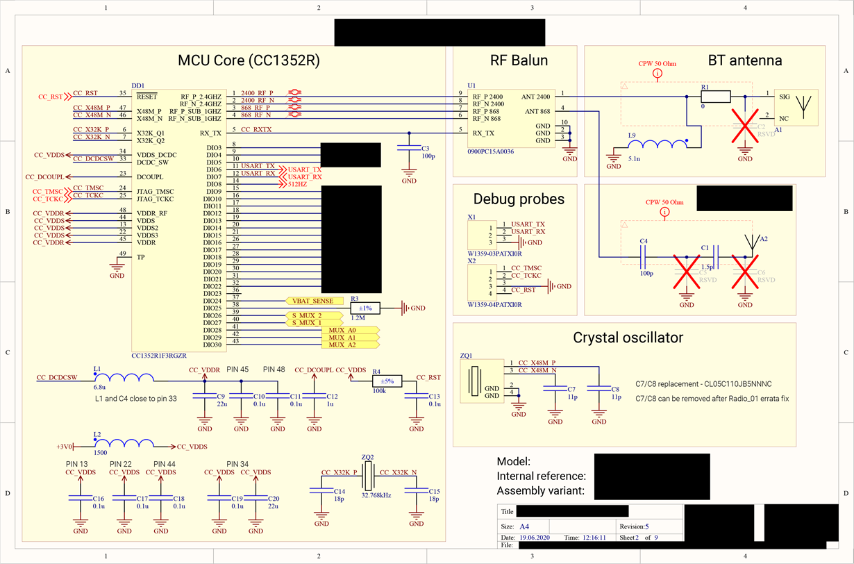
Schematic:

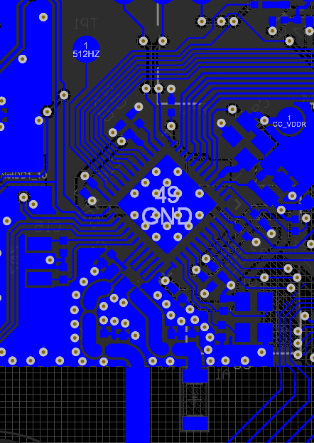
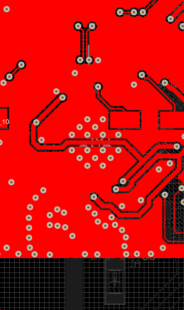
PCB views:

  • Hi,

    Refer to app note: https://www.ti.com/lit/an/swra629a

    What is the distance from the IPC to the chip (see Figure 9)?

    Track width ?

    The power routing on the bottom layer does not look too good and this divides the GND directly underneath the chip.

    Regards,

       Richard

  • 404 on that link. Been noticing a few in past days. Actual link is https://www.ti.com/lit/an/swra629a/swra629a.pdf

  • Hi, thanks for the reply.

    Distance between MCU and IPC is 1.07 mm, missed it a bit due to 45 angle placement. It isn't complicated to fix, but is it may be so critical (good to understand for future projects)?

    Track width between MCU and IPC is 0.2 mm, MCU to antenna is 1.02 mm (not 50 Ohm but the best I can get on 2-layer PCB). Power issue was discovered even before antennas, it's a direct output from the IPC.

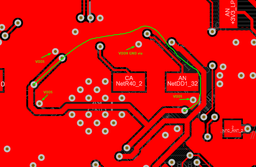
    Maybe you have some suggestions for power routing improvement (once again - it's 2-layer PCB)? I've decided to divide big pad so I could keep VDDS trace short enough and maintain short current loop from VDDS/VDDR capacitors to the MCU, wasn't sure if long VDDS trace is a good trade-off for keeping GND pad fully connected as it must be on 4L board. May try something like that:

  • Hi,

    I would keep the recommended distance between the IPC and the chip. Otherwise there will be phase shifts and this could cause a delta in output power and increased harmonics compared to the ref design. I do not believe this is the sole cause of losing 6 dB in output power.

    The power routing shown above is better since this does not divide the RF GND. I would route this signal outside the area of the GND pads of the decoupling caps so the return GND loop currents are kept to a minimum.

    We have not tested the CC1352 IPC on a 2-layer design since the majority of designs are 4-layers.

    Regards,

       Richard

  • Thank you for the hint, at least now I know what should I try :) I will write a comment after testing the PCB with rerouted power rails.

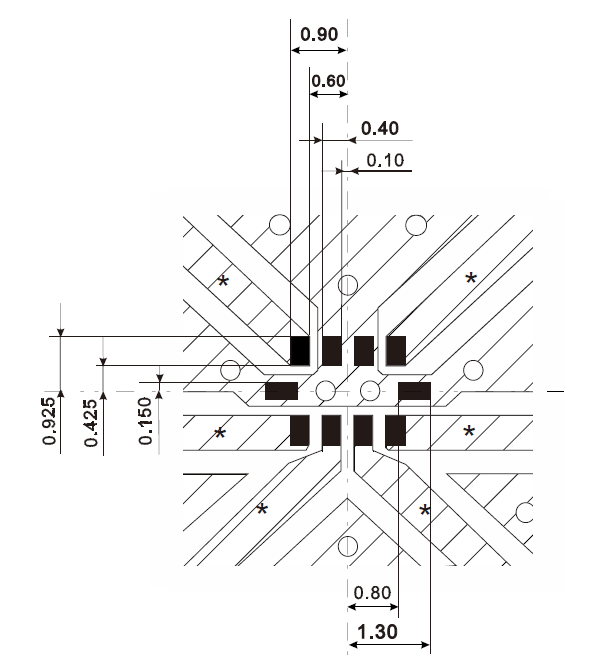
    One more question about the IPC. Datasheet from Johanson (https://www.johansontechnology.com/datasheets/0900PC15A0036/0900PC15A0036.pdf) tells to remove ground under the IPC:

    But your design (LPSTK-CC1352R) does have ground-reference pouring on top:

    Which variant is correct?

  • Hi,

    I would follow the original ref design that did not have GND underneath the IPC. Refer to figure 6 in app note: https://www.ti.com/lit/an/swra629a/swra629a.pdf

    LPSTCK-CC1352R has passed regulatory tests so this design works as well. 

    Regards,

       Richard

  • Hi,

    I've tested rerouted 2-layer PCB - around +2 dB improvement comparing to the previous version, but still 4 dB losses. I assumed that for proper result 4-layer PCB is a must, so tried to make a small 4-layer module (1.2mm total thickness, 0.2 mm prepreg), which can be soldered onto big 2-layer PCB. 2-layer PCB for that module still in development, but the module itself (on its evaluation board) shows good results - about 11 dB (plus ~0.5 dB losses for connectors between the module and antenna connector) at maximum Tx power, +2 dB improvement comparing with modified 2-layer PCB.

    I have one more question about the IPC.

    Received preliminary datasheet from Murata (LFB21868MDZ5E757), and was surprised to found that Murata's recommended land pattern differs from Johanson:

    From that, I guess that 0900PC15A0036 and LFB21868MDZ5E757 won't be compatible since they declare different land patterns (one does have GND underneath and another doesn't)?

    Have you evaluated Murata's part on your LPSTCK-CC1352R? Maybe difference from that GND may be neglected, plus Murata's document still has preliminary status, maybe that GND underneath is, in fact, a mistake :)

  • We have tested the IPC as described in https://www.ti.com/lit/an/swra629a/swra629a.pdf

    RGW is on vacation and will be back 17th August. He has followed up both Johanson and Murata so he has to comment on the different land pattern. As you see from the appnote the same pattern is used for both. 

  • Both IPCs have been tested on the TI QFN Evaluation Module.

    Each vendor has their own recommendations for the footprint so there can be a deltas between the two versions but both versions were qualified on the same TI QFN Evaluation Module.

  • Thanks for the remark about Murata.

    With MCU on 4-layer substrate we were able to achieve 11 dB @ sub-GHz output (from possible ~12-12.5, according to SWRA629A p.3.1.1), so I feel like I can close that topic now :)

    Thanks for your assistance!