- Ask a related questionWhat is a related question?A related question is a question created from another question. When the related question is created, it will be automatically linked to the original question.
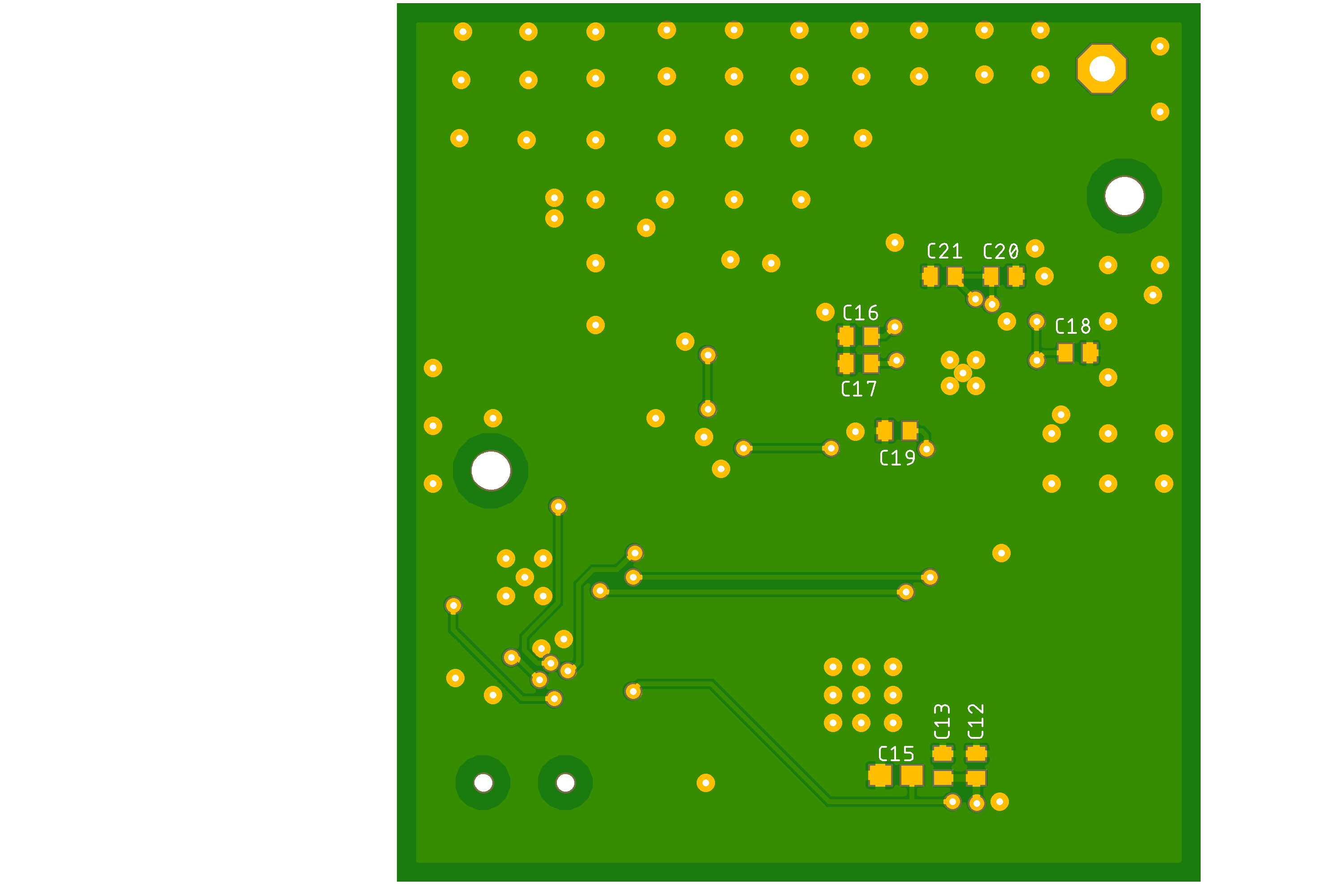
Hey, I'm new in RF design and would like to make a pcb with CC1101. I use esp32 micro controller and cp2102 in UART communication. All passive components are in 0402 packages, RF chip is connected via lines with 0.254 mm width, and 6 mil gaps between lines. In my production I'm gonna use FR-4 with 1.6mm thickness. I'm interested is it ok to have bypass capacitors on the bottom side and connected through vias? Also I looked at other boards and all of them use vias on the polygon, connected to the GND. What for they do this? and I placed vias too, is it ok? My aim to get 433 MHz transmitter/receiver