I'm studying this article now,
https://www.ti.com/lit/ug/swru458/swru458.pdf?ts=1623664712368
In the page 7,
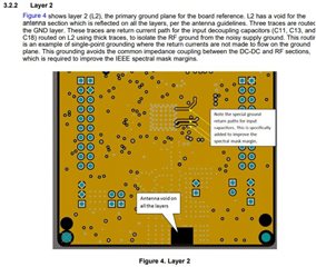
"3.2.2 Layer 2",
These traces are return current path for the input decoupling capacitors (C11, C13, and C18) routed on L2 using thick traces, to isolate the RF ground from the noisy supply ground.
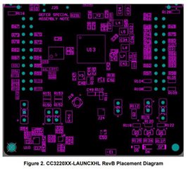
I'm trying to compare Figure 4 to the Figure 2, I cannot find C11, C13 and C18 having the relation to the return paths.
could you help confirm it?
Thanks.