Other Parts Discussed in Thread: WL1835,
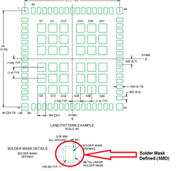
Currently, we are using wifi mod WL1835 in one of our designs. We are facing some shorting issues in between I/O pins after the reflow process. As per the attached datasheet, you have recommended SMD (Solder Mask Defined) pads for the footprint but in our design we have used NSMD (Non-Solder Mask Defined ) Pads, having land pattern data mentioned below,
FOR I/O PINS
1. Copper Pad (used in our design)---- 0.4mm X 0.75mm
Copper Pad (as per datasheet)---- Not defined in datasheet
2. Paste Pad (used in our design)---- 0.33mm X 0.75mm with Radius of 0.16mm
Paste Pad ( as per datasheet )---- 0.4mm X 0.75mm with Radius of 0.05mm
3. Open Solder Mask Pad (used in our design)---- 0.46mm X 0.81mm
Open Solder Mask ( as per datasheet )---- 0.4mm X 0.75mm
FOR 4 CORNER PADS
1. Copper Pad (used in our design)---- 0.75mm
Copper Pad (as per datasheet)---- not defined in datasheet
2. Paste Pad (used in our design)---- 0.52mm
Paste Pad ( as per datasheet )---- 0.713mm
3. Open Solder Mask Pad (used in our design)---- 0.8mm
Open Solder Mask ( as per datasheet )---- 0.75mm
FOR 36 THERMAL PADS
1. Copper Pad (used in our design)---- 1mm square pad
Copper Pad (as per datasheet)---- not defined in datasheet
2. Paste Pad (used in our design)---- 0.7 mm
Paste Pad ( as per datasheet )---- 0.95mm
3. Open Solder Mask Pad (used in our design)---- 1.06mm
Open Solder Mask ( as per datasheet )---- 1mm
Does NSMD pad create any shorting issue?? Or any other suggestion to avoid shorting issues between I/O pins? The shorting issue is happening between I/O pins only.