


Other Parts Discussed in Thread: SYSCONFIG
Hi!
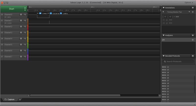
I'm currently using the SPI in master TX only mode and attempting to send data to my peripheral device. I have successfully been able to send the data if I set the minDMA transfer size to something really high (i.e. by not using the dma). I have also been able to send the data using a DMA if I set the mode to full-duplex mode. However, when I try to send data using the DMA in master Tx mode only, I can only send 33 bytes after it hangs. To be clear, the mcu doesn't seem to crash (if I have a timeout for the spi, I can see the program continues to execute), the data just isn't being sent. I'm a little lost on what to try next since this seems like an Ti driver issue. I have the register state after the device spi stop working, and I have attached a picture of what the output looks like.
HL_REV	0x40300A0B	IP Revision Identifier (X.Y.R) Used by software to track features bugs and compatibility [Memory Mapped]
	SCHEME	01
	RSVD	00	Reserved These bits are initialized to zero and writes to them are ignored.
	FUNC	000000110000	Function indicates a software compatible module family. If there is no level of software compatibility a new Func number (and hence REVISION) should be assigned.
	R_RTL	00001	RTL Version (R) maintained by IP design owner. RTL follows a numbering such as X.Y.R.Z which are explained in this table. R changes ONLY when: (1) PDS uploads occur which may have been due to spec changes (2) Bug fixes occur (3) Resets to '0' when X or Y changes. Design team has an internal 'Z' (customer invisible) number which increments on every drop that happens due to DV and RTL updates. Z resets to 0 when R increments.
	X_MAJOR	010	Major Revision (X) maintained by IP specification owner. X changes ONLY when: (1) There is a major feature addition. An example would be adding Master Mode to Utopia Level2. The Func field (or Class/Type in old PID format) will remain the same. X does NOT change due to: (1) Bug fixes (2) Change in feature parameters.
	CUSTOM	00
	Y_MINOR	001011	Minor Revision (Y) maintained by IP specification owner. Y changes ONLY when: (1) Features are scaled (up or down). Flexibility exists in that this feature scalability may either be represented in the Y change or a specific register in the IP that indicates which features are exactly available. (2) When feature creeps from Is-Not list to Is list. But this may not be the case once it sees silicon; in which case X will change. Y does NOT change due to: (1) Bug fixes (2) Typos or clarifications (3) major functional/feature change/addition/deletion. Instead these changes may be reflected via R S X as applicable. Spec owner maintains a customer-invisible number 'S' which changes due to: (1) Typos/clarifications (2) Bug documentation. Note that this bug is not due to a spec change but due to implementation. Nevertheless the spec tracks the IP bugs. An RTL release (say for silicon PG1.1) that occurs due to bug fix should document the corresponding spec number (X.Y.S) in its release notes.
HL_HWINFO	0x00000009	Information about the IP module's hardware configuration i.e. typically the module's HDL generics (if any). Actual field format and encoding is up to the module's designer to decide. [Memory Mapped]
	FFNBYTE	00100
HL_SYSCONFIG	0x00000008	0x4402 1010 0x4402 2010 Clock management configuration [Memory Mapped]
	IDLEMODE	10	Configuration of the local target state management mode. By definition target can handle read/write transaction as long as it is out of IDLE state. 0x0 Force-idle mode: local target's idle state follows (acknowledges) the system's idle requests unconditionally i.e. regardless of the IP module's internal requirements.Backup mode for debug only. 0x1 No-idle mode: local target never enters idle state.Backup mode for debug only. 0x2 Smart-idle mode: local target's idle state eventually follows (acknowledges) the system's idle requests depending on the IP module's internal requirements.IP module shall not generate (IRQ- or DMA-request-related) wakeup events. 0x3 "Smart-idle wakeup-capable mode: local target's idle state eventually follows (acknowledges) the system's idle requests depending on the IP module's internal requirements.IP module may generate (IRQ- or DMA-request-related) wakeup events when in idle state.Mode is only relevant if the appropriate IP module ""swakeup"" output(s) is (are) implemented."
REVISION	0x0000002B	0x4402 1100 0x4402 2100 This register contains the hard coded RTL revision number. [Memory Mapped]
	REV	00101011	IP revision [7:4] Major revision [3:0] Minor revision Examples: 0x10 for 1.0 0x21 for 2.1
SYSCONFIG	0x00000015	0x4402 1110 0x4402 2110 This register allows controlling various parameters of the OCP interface. [Memory Mapped]
	CLOCKACTIVITY	00	Clocks activity during wake up mode period 0x0 OCP and Functional clocks may be switched off. 0x1 OCP clock is maintained. Functional clock may be switched-off. 0x2 Functional clock is maintained. OCP clock may be switched-off. 0x3 OCP and Functional clocks are maintained.
	SIDLEMODE	10	Power management 0x0 If an idle request is detected the McSPI acknowledges it unconditionally and goes in Inactive mode. Interrupt DMA requests and wake up lines are unconditionally de-asserted and the module wakeup capability is deactivated even if the bit MCSPI_SYSCONFIG[EnaWakeUp] is set. 0x1 If an idle request is detected the request is ignored and the module does not switch to wake up mode and keeps on behaving normally. 0x2 If an idle request is detected the module will switch to idle mode based on its internal activity. The wake up capability cannot be used. 0x3 If an idle request is detected the module will switch to idle mode based on its internal activity and the wake up capability can be used if the bit MCSPI_SYSCONFIG[EnaWakeUp] is set.
SYSSTATUS	0x00000001	0x4402 1114 0x4402 2114 This register provides status information about the module excluding the interrupt status information [Memory Mapped]
IRQSTATUS	0x00000004	0x4402 1118 0x4402 2118 The interrupt status regroups all the status of the module internal events that can generate an interrupt [Memory Mapped]
IRQENABLE	0x00000000	0x4402 111C 0x4402 211C This register allows to enable/disable the module internal sources of interrupt on an event-by-event basis. [Memory Mapped]
WAKEUPENABLE	0x00000000	0x4402 1120 0x4402 2120 The wakeup enable register allows to enable/disable the module internal sources of wakeup on event-by-event basis. [Memory Mapped]
SYST	0x00000000	0x4402 1124 0x4402 2124 This register is used to check the correctness of the system interconnect either internally to peripheral bus or externally to device IO pads when the module is configured in system test (SYSTEST) mode. [Memory Mapped]
MODULCTRL	0x00000003	0x4402 1128 0x4402 2128 This register is dedicated to the configuration of the serial port interface. [Memory Mapped]
	INITDLY	000	Initial spi delay for first transfer: This register is an option only available in SINGLE master mode The controller waits for a delay to transmit the first spi word after channel enabled and corresponding TX register filled. This Delay is based on SPI output frequency clock No clock output provided to the boundary and chip select is not active in 4 pin mode within this period. 0x0 No delay for first spi transfer. 0x1 The controller wait 4 spi bus clock 0x2 The controller wait 8 spi bus clock 0x3 The controller wait 16 spi bus clock 0x4 The controller wait 32 spi bus clock
CH0CONF	0x381143F8	0x4402 112C 0x4402 212C This register is dedicated to the configuration of the channel 0 [Memory Mapped]
	TCS0	00	Chip Select Time Control This 2-bits field defines the number of interface clock cycles between CS toggling and first or last edge of SPI clock. 0x0 0.5 clock cycle 0x1 1.5 clock cycle 0x2 2.5 clock cycle 0x3 3.5 clock cycle
	SPIENSLV	00	Channel 0 only and slave mode only: SPI slave select signal detection. Reserved bits for other cases. 0x0 Detection enabled only on SPIEN[0] 0x1 Detection enabled only on SPIEN[1] 0x2 Detection enabled only on SPIEN[2] 0x3 Detection enabled only on SPIEN[3]
	TRM	00	Transmit/Receive modes 0x0 Transmit and Receive mode 0x1 Receive only mode 0x2 Transmit only mode 0x3 Reserved
	WL	00111	SPI word length 0x00 Reserved 0x01 Reserved 0x02 Reserved 0x03 The SPI word is 4-bits long 0x04 The SPI word is 5-bits long 0x05 The SPI word is 6-bits long 0x06 The SPI word is 7-bits long 0x07 The SPI word is 8-bits long 0x08 The SPI word is 9-bits long 0x09 The SPI word is 10-bits long 0x0A The SPI word is 11-bits long 0x0B The SPI word is 12-bits long 0x0C The SPI word is 13-bits long 0x0D The SPI word is 14-bits long 0x0E The SPI word is 15-bits long 0x0F The SPI word is 16-bits long 0x10 The SPI word is 17-bits long 0x11 The SPI word is 18-bits long 0x12 The SPI word is 19-bits long 0x13 The SPI word is 20-bits long 0x14 The SPI word is 21-bits long 0x15 The SPI word is 22-bits long 0x16 The SPI word is 23-bits long 0x17 The SPI word is 24-bits long 0x18 The SPI word is 25-bits long 0x19 The SPI word is 26-bits long 0x1A The SPI word is 27-bits long 0x1B The SPI word is 28-bits long 0x1C The SPI word is 29-bits long 0x1D The SPI word is 30-bits long 0x1E The SPI word is 31-bits long 0x1F The SPI word is 32-bits long
	CLKD	1110	Frequency divider for SPICLK. (only when the module is a Master SPI device). A programmable clock divider divides the SPI reference clock (CLKSPIREF) with a 4-bit value and results in a new clock SPICLK available to shift-in and shift-out data. By default the clock divider ratio has a power of two granularity when MCSPI_CHCONF[CLKG] is cleared Otherwise this register is the 4 LSB bit of a 12-bit register concatenated with clock divider extension MCSPI_CHCTRL[EXTCLK] register.The value description below defines the clock ratio when MCSPI_CHCONF[CLKG] is set to 0. 0x0 1 0x1 2 0x2 4 0x3 8 0x4 16 0x5 32 0x6 64 0x7 128 0x8 256 0x9 512 0xA 1024 0xB 2048 0xC 4096 0xD 8192 0xE 16384 0xF 32768
CH0STAT	0x00000057	0x4402 1130 0x4402 2130 This register provides status information about transmitter and receiver registers of channel 0 [Memory Mapped]
CH0CTRL	0x00000001	0x4402 1134 0x4402 2134 This register is dedicated to enable the channel 0 [Memory Mapped]
	EXTCLK	00000000	Clock ratio extension: This register is used to concatenate with MCSPI_CHCONF[CLKD] register for clock ratio only when granularity is one clock cycle (MCSPI_CHCONF[CLKG] set to 1). Then the max value reached is 4096 clock divider ratio. 0x00 Clock ratio is CLKD + 1 0x01 Clock ratio is CLKD + 1 + 16 0xFF Clock ratio is CLKD + 1 + 4080
TX0	0x00000041	0x4402 1138 0x4402 2138 This register contains a single SPI word to transmit on the serial link what ever SPI word length is. [Memory Mapped]
RX0	0x00000000	0x4402 113C 0x4402 213C This register contains a single SPI word received through the serial link what ever SPI word length is. [Memory Mapped]
CH1CONF	0x00060000	0x4402 1140 0x4402 2140 This register is dedicated to the configuration of the channel. [Memory Mapped]
	TCS1	00	Chip Select Time Control This 2-bits field defines the number of interface clock cycles between CS toggling and first or last edge of SPI clock. 0x0 0.5 clock cycle 0x1 1.5 clock cycle 0x2 2.5 clock cycle 0x3 3.5 clock cycle
	TRM	00	Transmit/Receive modes 0x0 Transmit and Receive mode 0x1 Receive only mode 0x2 Transmit only mode 0x3 Reserved
	WL	00000	SPI word length 0x00 Reserved 0x01 Reserved 0x02 Reserved 0x03 The SPI word is 4-bits long 0x04 The SPI word is 5-bits long 0x05 The SPI word is 6-bits long 0x06 The SPI word is 7-bits long 0x07 The SPI word is 8-bits long 0x08 The SPI word is 9-bits long 0x09 The SPI word is 10-bits long 0x0A The SPI word is 11-bits long 0x0B The SPI word is 12-bits long 0x0C The SPI word is 13-bits long 0x0D The SPI word is 14-bits long 0x0E The SPI word is 15-bits long 0x0F The SPI word is 16-bits long 0x10 The SPI word is 17-bits long 0x11 The SPI word is 18-bits long 0x12 The SPI word is 19-bits long 0x13 The SPI word is 20-bits long 0x14 The SPI word is 21-bits long 0x15 The SPI word is 22-bits long 0x16 The SPI word is 23-bits long 0x17 The SPI word is 24-bits long 0x18 The SPI word is 25-bits long 0x19 The SPI word is 26-bits long 0x1A The SPI word is 27-bits long 0x1B The SPI word is 28-bits long 0x1C The SPI word is 29-bits long 0x1D The SPI word is 30-bits long 0x1E The SPI word is 31-bits long 0x1F The SPI word is 32-bits long
	CLKD	0000	Frequency divider for SPICLK. (only when the module is a Master SPI device). A programmable clock divider divides the SPI reference clock (CLKSPIREF) with a 4-bit value and results in a new clock SPICLK available to shift-in and shift-out data. By default the clock divider ratio has a power of two granularity when MCSPI_CHCONF[CLKG] is cleared Otherwise this register is the 4 LSB bit of a 12-bit register concatenated with clock divider extension MCSPI_CHCTRL[EXTCLK] register.The value description below defines the clock ratio when MCSPI_CHCONF[CLKG] is set to 0. 0x0 1 0x1 2 0x2 4 0x3 8 0x4 16 0x5 32 0x6 64 0x7 128 0x8 256 0x9 512 0xA 1024 0xB 2048 0xC 4096 0xD 8192 0xE 16384 0xF 32768
CH1STAT	0x00000000	0x4402 1144 0x4402 2144 This register provides status information about transmitter and receiver registers of channel 1 [Memory Mapped]
CH1CTRL	0x00000000	0x4402 1148 0x4402 2148 This register is dedicated to enable the channel 1 [Memory Mapped]
	EXTCLK	00000000	Clock ratio extension: This register is used to concatenate with MCSPI_CHCONF[CLKD] register for clock ratio only when granularity is one clock cycle (MCSPI_CHCONF[CLKG] set to 1). Then the max value reached is 4096 clock divider ratio. 0x00 Clock ratio is CLKD + 1 0x01 Clock ratio is CLKD + 1 + 16 0xFF Clock ratio is CLKD + 1 + 4080
TX1	0x00000000	0x4402 114C 0x4402 214C This register contains a single SPI word to transmit on the serial link what ever SPI word length is. [Memory Mapped]
RX1	0x00000000	0x4402 1150 0x4402 2150 This register contains a single SPI word received through the serial link what ever SPI word length is. [Memory Mapped]
CH2CONF	0x00060000	0x4402 1154 0x4402 2154 This register is dedicated to the configuration of the channel 2 [Memory Mapped]
	TCS2	00	Chip Select Time Control This 2-bits field defines the number of interface clock cycles between CS toggling and first or last edge of SPI clock. 0x0 0.5 clock cycle 0x1 1.5 clock cycle 0x2 2.5 clock cycle 0x3 3.5 clock cycle
	TRM	00	Transmit/Receive modes 0x0 Transmit and Receive mode 0x1 Receive only mode 0x2 Transmit only mode 0x3 Reserved
	WL	00000	SPI word length 0x00 Reserved 0x01 Reserved 0x02 Reserved 0x03 The SPI word is 4-bits long 0x04 The SPI word is 5-bits long 0x05 The SPI word is 6-bits long 0x06 The SPI word is 7-bits long 0x07 The SPI word is 8-bits long 0x08 The SPI word is 9-bits long 0x09 The SPI word is 10-bits long 0x0A The SPI word is 11-bits long 0x0B The SPI word is 12-bits long 0x0C The SPI word is 13-bits long 0x0D The SPI word is 14-bits long 0x0E The SPI word is 15-bits long 0x0F The SPI word is 16-bits long 0x10 The SPI word is 17-bits long 0x11 The SPI word is 18-bits long 0x12 The SPI word is 19-bits long 0x13 The SPI word is 20-bits long 0x14 The SPI word is 21-bits long 0x15 The SPI word is 22-bits long 0x16 The SPI word is 23-bits long 0x17 The SPI word is 24-bits long 0x18 The SPI word is 25-bits long 0x19 The SPI word is 26-bits long 0x1A The SPI word is 27-bits long 0x1B The SPI word is 28-bits long 0x1C The SPI word is 29-bits long 0x1D The SPI word is 30-bits long 0x1E The SPI word is 31-bits long 0x1F The SPI word is 32-bits long
	CLKD	0000	Frequency divider for SPICLK. (only when the module is a Master SPI device). A programmable clock divider divides the SPI reference clock (CLKSPIREF) with a 4-bit value and results in a new clock SPICLK available to shift-in and shift-out data. By default the clock divider ratio has a power of two granularity when MCSPI_CHCONF[CLKG] is cleared Otherwise this register is the 4 LSB bit of a 12-bit register concatenated with clock divider extension MCSPI_CHCTRL[EXTCLK] register.The value description below defines the clock ratio when MCSPI_CHCONF[CLKG] is set to 0. 0x0 1 0x1 2 0x2 4 0x3 8 0x4 16 0x5 32 0x6 64 0x7 128 0x8 256 0x9 512 0xA 1024 0xB 2048 0xC 4096 0xD 8192 0xE 16384 0xF 32768
CH2STAT	0x00000000	0x4402 1158 0x4402 2158 This register provides status information about transmitter and receiver registers of channel 2 [Memory Mapped]
CH2CTRL	0x00000000	0x4402 115C 0x4402 215C This register is dedicated to enable the channel 2 [Memory Mapped]
	EXTCLK	00000000	Clock ratio extension: This register is used to concatenate with MCSPI_CHCONF[CLKD] register for clock ratio only when granularity is one clock cycle (MCSPI_CHCONF[CLKG] set to 1). Then the max value reached is 4096 clock divider ratio. 0x00 Clock ratio is CLKD + 1 0x01 Clock ratio is CLKD + 1 + 16 0xFF Clock ratio is CLKD + 1 + 4080
TX2	0x00000000	0x4402 1160 0x4402 2160 This register contains a single SPI word to transmit on the serial link what ever SPI word length is. [Memory Mapped]
RX2	0x00000000	0x4402 1164 0x4402 2164 This register contains a single SPI word received through the serial link what ever SPI word length is. [Memory Mapped]
CH3CONF	0x00060000	0x4402 1168 0x4402 2168 This register is dedicated to the configuration of the channel 3 [Memory Mapped]
	TCS3	00	Chip Select Time Control This 2-bits field defines the number of interface clock cycles between CS toggling and first or last edge of SPI clock. 0x0 0.5 clock cycle 0x1 1.5 clock cycle 0x2 2.5 clock cycle 0x3 3.5 clock cycle
	TRM	00	Transmit/Receive modes 0x0 Transmit and Receive mode 0x1 Receive only mode 0x2 Transmit only mode 0x3 Reserved
	WL	00000	SPI word length 0x00 Reserved 0x01 Reserved 0x02 Reserved 0x03 The SPI word is 4-bits long 0x04 The SPI word is 5-bits long 0x05 The SPI word is 6-bits long 0x06 The SPI word is 7-bits long 0x07 The SPI word is 8-bits long 0x08 The SPI word is 9-bits long 0x09 The SPI word is 10-bits long 0x0A The SPI word is 11-bits long 0x0B The SPI word is 12-bits long 0x0C The SPI word is 13-bits long 0x0D The SPI word is 14-bits long 0x0E The SPI word is 15-bits long 0x0F The SPI word is 16-bits long 0x10 The SPI word is 17-bits long 0x11 The SPI word is 18-bits long 0x12 The SPI word is 19-bits long 0x13 The SPI word is 20-bits long 0x14 The SPI word is 21-bits long 0x15 The SPI word is 22-bits long 0x16 The SPI word is 23-bits long 0x17 The SPI word is 24-bits long 0x18 The SPI word is 25-bits long 0x19 The SPI word is 26-bits long 0x1A The SPI word is 27-bits long 0x1B The SPI word is 28-bits long 0x1C The SPI word is 29-bits long 0x1D The SPI word is 30-bits long 0x1E The SPI word is 31-bits long 0x1F The SPI word is 32-bits long
	CLKD	0000	Frequency divider for SPICLK. (only when the module is a Master SPI device). A programmable clock divider divides the SPI reference clock (CLKSPIREF) with a 4-bit value and results in a new clock SPICLK available to shift-in and shift-out data. By default the clock divider ratio has a power of two granularity when MCSPI_CHCONF[CLKG] is cleared Otherwise this register is the 4 LSB bit of a 12-bit register concatenated with clock divider extension MCSPI_CHCTRL[EXTCLK] register.The value description below defines the clock ratio when MCSPI_CHCONF[CLKG] is set to 0. 0x0 1 0x1 2 0x2 4 0x3 8 0x4 16 0x5 32 0x6 64 0x7 128 0x8 256 0x9 512 0xA 1024 0xB 2048 0xC 4096 0xD 8192 0xE 16384 0xF 32768
CH3STAT	0x00000000	0x4402 116C 0x4402 216C This register provides status information about transmitter and receiver registers of channel 3 [Memory Mapped]
CH3CTRL	0x00000000	0x4402 1170 0x4402 2170 This register is dedicated to enable the channel 3 [Memory Mapped]
	EXTCLK	00000000	Clock ratio extension: This register is used to concatenate with MCSPI_CHCONF[CLKD] register for clock ratio only when granularity is one clock cycle (MCSPI_CHCONF[CLKG] set to 1). Then the max value reached is 4096 clock divider ratio. 0x00 Clock ratio is CLKD + 1 0x01 Clock ratio is CLKD + 1 + 16 0xFF Clock ratio is CLKD + 1 + 4080
TX3	0x00000000	0x4402 1174 0x4402 2174 This register contains a single SPI word to transmit on the serial link what ever SPI word length is. [Memory Mapped]
RX3	0x00000000	0x4402 1178 0x4402 2178 This register contains a single SPI word received through the serial link what ever SPI word length is. [Memory Mapped]
XFERLEVEL	0x03C40000	0x4402 117C 0x4402 217C This register provides transfer levels needed while using FIFO buffer during transfer. [Memory Mapped]
	WCNT	0000001111000100	Spi word counterThis register holds the programmable value of number of SPI word to be transferred on channel which is using the FIFO buffer.When transfer had started a read back in this register returns the current SPI word transfer index. 0x0000 Counter not used 0x0001 one word 0xFFFE 65534 spi word 0xFFFF 65535 spi word
	AFL	00000000	Buffer Almost Full This register holds the programmable almost full level value used to determine almost full buffer condition. If the user wants an interrupt or a DMA read request to be issued during a receive operation when the data buffer holds at least n bytes then the buffer MCSPI_MODULCTRL[AFL] must be set with n-1.The size of this register is defined by the generic parameter FFNBYTE. 0x00 one byte 0x01 2 bytes 0xFE 255bytes 0xFF 256bytes
	AEL	00000000	Buffer Almost EmptyThis register holds the programmable almost empty level value used to determine almost empty buffer condition. If the user wants an interrupt or a DMA write request to be issued during a transmit operation when the data buffer is able to receive n bytes then the buffer MCSPI_MODULCTRL[AEL] must be set with n-1. 0x00 one byte 0x01 2 bytes 0xFE 255 bytes 0xFF 256bytes
DAFTX	0x00000000	0x4402 1180 0x4402 2180 This register contains the SPI words to transmit on the serial link when FIFO used and DMA address is aligned on 256 bit.This register is an image of one of MCSPI_TX(i) register corresponding to the channel which have its FIFO enabled. [Memory Mapped]
DAFRX	0x00000000	0x4402 11A0 0x4402 21A0 This register contains the SPI words to received on the serial link when FIFO used and DMA address is aligned on 256 bit.This register is an image of one of MCSPI_RX(i) register corresponding to the channel which have its FIFO enabled. **************************************************************************** [Memory Mapped]


STAT	0x001F0001	Memory Mapped
	DMACHANS	11111	Available uDMA Channels Minus 1
	STATE	0000	Control State Machine Status 0x00000090 : UDMA_STAT_STATE_DONE : Done 0x00000000 : UDMA_STAT_STATE_IDLE : Idle 0x00000010 : UDMA_STAT_STATE_RD_CTRL : Reading channel controller data 0x00000030 : UDMA_STAT_STATE_RD_DSTENDP : Reading destination end pointer 0x00000040 : UDMA_STAT_STATE_RD_SRCDAT : Reading source data 0x00000020 : UDMA_STAT_STATE_RD_SRCENDP : Reading source end pointer 0x00000080 : UDMA_STAT_STATE_STALL : Stalled 0x000000A0 : UDMA_STAT_STATE_UNDEF : Undefined 0x00000060 : UDMA_STAT_STATE_WAIT : Waiting for uDMA request to clear 0x00000070 : UDMA_STAT_STATE_WR_CTRL : Writing channel controller data 0x00000050 : UDMA_STAT_STATE_WR_DSTDAT : Writing destination data
CFG	0x00000000	Memory Mapped
CTLBASE	0x2000CC00	Memory Mapped
	ADDR	0010000000000000110011	Channel Control Base Address
ALTBASE	0x2000CE00	Memory Mapped
WAITSTAT	0x00000F00	Memory Mapped
SWREQ	0x00000000	Memory Mapped
USEBURSTSET	0x00000000	Memory Mapped
USEBURSTCLR	0x00000000	Memory Mapped
REQMASKSET	0x00000000	Memory Mapped
REQMASKCLR	0x00000000	Memory Mapped
ENASET	0x80000001	Memory Mapped
ENACLR	0x80000001	Memory Mapped
ALTSET	0x00000000	Memory Mapped
ALTCLR	0x00000000	Memory Mapped
PRIOSET	0x00000000	Memory Mapped
PRIOCLR	0x00000000	Memory Mapped
ERRCLR	0x00000000	Memory Mapped
CHASGN	0x40000000	Memory Mapped
CHIS	0x00000000	Memory Mapped
CHMAP0	0x00000000	Memory Mapped
	CH7SEL	0000	uDMA Channel 7 Source Select
	CH6SEL	0000	uDMA Channel 6 Source Select
	CH5SEL	0000	uDMA Channel 5 Source Select
	CH4SEL	0000	uDMA Channel 4 Source Select
	CH3SEL	0000	uDMA Channel 3 Source Select
	CH2SEL	0000	uDMA Channel 2 Source Select
	CH1SEL	0000	uDMA Channel 1 Source Select
	CH0SEL	0000	uDMA Channel 0 Source Select
CHMAP1	0x00000000	Memory Mapped
	CH15SEL	0000	uDMA Channel 15 Source Select
	CH14SEL	0000	uDMA Channel 14 Source Select
	CH13SEL	0000	uDMA Channel 13 Source Select
	CH12SEL	0000	uDMA Channel 12 Source Select
	CH11SEL	0000	uDMA Channel 11 Source Select
	CH10SEL	0000	uDMA Channel 10 Source Select
	CH9SEL	0000	uDMA Channel 9 Source Select
	CH8SEL	0000	uDMA Channel 8 Source Select
CHMAP2	0x00000000	Memory Mapped
	CH23SEL	0000	uDMA Channel 23 Source Select
	CH22SEL	0000	uDMA Channel 22 Source Select
	CH21SEL	0000	uDMA Channel 21 Source Select
	CH20SEL	0000	uDMA Channel 20 Source Select
	CH19SEL	0000	uDMA Channel 19 Source Select
	CH18SEL	0000	uDMA Channel 18 Source Select
	CH17SEL	0000	uDMA Channel 17 Source Select
	CH16SEL	0000	uDMA Channel 16 Source Select
CHMAP3	0x03000000	Memory Mapped
	CH31SEL	0000	uDMA Channel 31 Source Select
	CH30SEL	0011	uDMA Channel 30 Source Select
	CH29SEL	0000	uDMA Channel 29 Source Select
	CH28SEL	0000	uDMA Channel 28 Source Select
	CH27SEL	0000	uDMA Channel 27 Source Select
	CH26SEL	0000	uDMA Channel 26 Source Select
	CH25SEL	0000	uDMA Channel 25 Source Select
	CH24SEL	0000	uDMA Channel 24 Source Select
PV	0x00000000	Memory Mapped
	MAJOR	00000000	Major Revision
	MINOR	00000000	Minor Revision
Any help is appreciated!
Thanks!
Vasav


