This thread has been locked.

If you have a related question, please click the "Ask a related question" button in the top right corner. The newly created question will be automatically linked to this question.

WL1837MOD: Calibrator RSSI questions

Part Number: WL1837MOD
Other Parts Discussed in Thread: , WL1837

I have a couple questions related to the calibrator tool. Hopefully easy questions. Again, I am talking about this document/feature.


https://www.ti.com/lit/ug/swru562/swru562.pdf?ts=1653527288951


My first question is about the get_rx_stats output (shown below).


RX statistics (status 0)

Total Received Packets: 8341

FCS Errors:             747

MAC Mismatch:           0

Good Packets:           7594

Average RSSI (SOC):     -75

Average RSSI (ANT):     -72

PER:                    0.089558     # PER = Total Bad / Total Received


Most of it make sense, but what is the difference between Average RSSI (SOC) and Average RSSI (ANT)? They are consistently 3dB apart. Maybe you will answer this within the first answer, but why 3dB?


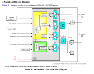
Next question, also it may be answered within the first answer, but which RSSI (SOC or ANT) corresponds to the data within the datasheet (shown below).

How do I see RSSI for each Antenna as ours is 2x2 MIMO

  • Brad,

    I believe RSSI ANT is RSSI @ the antenna end and RSSI SoC is RSSI @ the SoC end which would be less considering antenna trace loss etc. 

    As per wl1837MOD datasheet  section 8 "All specifications are measured at the module pins using the TI WL1837MODCOM8I evaluation board. All measurements are performed with VBAT = 3.7 V, VIO = 1.8 V, 25°C for typical values with matched RF antennas" . It should be RSSI @ the antenna . 

    I don't believe PLT will display RSSI for each antenna in MIMO mode - it will display one RSSI value ( just like datasheet )

    Also , I have copied h/w expert to make any additional comments if needed

    SN

  • As per the Functional Block Diagram below

    what we are buying is the module which has the WL1837 chipset, which is the yellow block above right, that is the SOC, and there is Power Amplifier in TX chain and LNA on the RX side and then comes the Antenna connector which is at the edge of the module as pin as RF_ANT1(PIN 32) and RF_ANT2(PIN 18)

    So the RSSI shown in the Average RSSI (SOC):  is at the yellow block ?

    Average RSSI (ANT): is at the RF_ANT1(pin 32)?

    why fixed 3dB difference, is is the Attenuation from RF_ANTx to the SOC pin ?

    when we use this module, we are soldering it on our PCBA, so the PIN 32(RF_ANT1) and PIN 18(RF_ANT2) is connected to the PCB track and then connected to the RF Antenna port on our PCBA. 

    so when we measure the Tx Power and Rx Sensitivity, we will be getting less Tx Power and Rx sensitivity will be more right ? so what parameters we should be adjusting it in the ini files?

  • Hello Dino,

    In the block diagram, the grey box is the chipset. The PA and LNA are internal to the IC.

    Internal to the module on the RF path from the IC to the module RF pins are a switch, filters, and diplexer. The insertion loss of these components add up to 3dB.

    It is advised not to make any modifications to the INI in order to pass regulatory certification tests. 

    BR,

    Seong