This thread has been locked.

If you have a related question, please click the "Ask a related question" button in the top right corner. The newly created question will be automatically linked to this question.

CC3135: Design 50Ohm PCB traces

Part Number: CC3135

Dear all

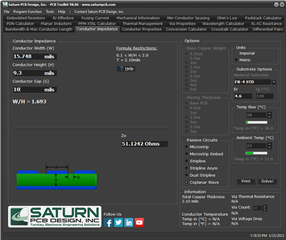
To ensure the RF path is designed with an impedance of 50 Ω I calculated the track with 400um. Just before I hand it to layouter, could anyone tell me if I'm on the good side or if it's completely off, what I get? 

My Stack up is

CU Top: 35um

FR-4: 0.236mm

CU M1: 70um (needed for high current)

FR-4: 0.868mm

CU M2: 70um (needed for high current)

FR-4: 0.236mm

CU Bottom: 35um

Is the track with of 400um reasonable?

Shall I guard the track with Vias all the way?

Are there any restrictions for the length of that line (I intend to have about 10mm - 20mm)

Any help appreciated. Many thanks 

Chris

  • Hi Chris,

    First of all I highly recommend you look at our existing documentation the CC3x35 SimpleLink Wi-Fi® and IoT solution layout guidelines. This User guide explains the design guidelines for designing a board for the CC3135 and CC3235 to optimize the performance of the board.  It is also important to verify the schematic by going through our CC3x35 Hardware Design Checklist, Lastly once you have finished your design you can request a HW review at https://www.ti.com/tool/SIMPLELINK-WIFI-DESIGN-REVIEWS.  

    Just before I hand it to layouter, could anyone tell me if I'm on the good side or if it's completely off, what I get? 

    It is hard to know with the information you provided, by assuming a few values it seems to be alright.  Although note that calculating the impedance will not ensure that the impedance is 50ohms, which is why we recommend to place place pi matching components in your design. 

    Using a tool called "Saturn PCB toolkit" the estimated impedance seems to be 51.1242 ohms (see image below), but that was assuming a Dielectric constant of 4.6 and a 10mil gap.

    Are there any restrictions for the length of that line (I intend to have about 10mm - 20mm)

    The length of the transmission line should not affect the RF much, but it must have impedance matching of 50ohms.  It is recommended to implement Impedance matching networks to ensure continuous 50 ohms impedance. (refer to section 4.1.6 Impedance Matching of the Layout Guide).

    Is the track with of 400um reasonable?

    The transmission line being 15.748 mils could be fine, although our reference design uses 16.7 mils ( 424.18um). We base our designs with the "coplanar waveguide with ground" (CPW-G) structure. Then estimated values of the impedance and other values are done with tools like AWR TX Line, Saturn PCB Toolkit, and Agilent ADS.

    Shall I guard the track with Vias all the way?

    We recommend to use via stitching along the RF trace to reduce emissions, and keep the fields confined to the trace boundary. As such do place ground vias along the transmission line when feasible.  

    Let me know if you have any other related questions.

    BR,

    Jessica M. Torres