This thread has been locked.

If you have a related question, please click the "Ask a related question" button in the top right corner. The newly created question will be automatically linked to this question.

CC3220S-LAUNCHXL: external power to the launchpad

Part Number: CC3220S-LAUNCHXL
Other Parts Discussed in Thread: CC3220S, , CC3220SF, SYSCONFIG, UNIFLASH, CC3220R, CC3235S

Hi

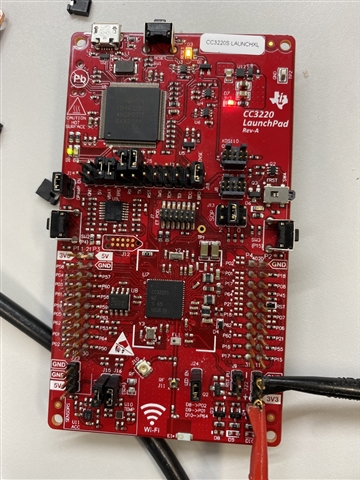
I have the CC3220S launchpad.

When i power the board using the 3.3V pin with all the jumpers as per the CC3220 SimpleLinkTm Wi-Fi® LaunchPadTm Development
Kit Hardware (swru463c of mar2020) i find that the WiFi does not operate...in fact, i suspect my program is stuck waiting for the return from the network/radio processor.
(The scope shows that both the 32KHz & 40MHz oscillators are oscillating correctly)

However, when i power the board using the 5V pin (with the jumpers suitably repositioned), i find that EVERYTHING functions correctly. 

My question is...why does the CC3220 section of the launchpad not function correctly/completely at 3.3.V???

thanks 

  • Hi Moshe,

    Could you inform me on which board revision of the CC3220S-LAUNCHXL you are using? Can you also list the jumpers you are repositioning when switching from 5V to 3.3V?

  • Hi Andy

    I have Rev-A

    For 5V i jumper J20 (5V), J19 (VBAT), J17 (BRD), J5 (RST) & J8 (VSENSE).....J21 & J3 are unjumpered.

    For 3.3V i unjumper all the above but jumper J17 to J19 on their pin 1s (pin closer to the CC3220 chip) . I also jumper J9.

  • Moshe,

    Are you using the on board XDS110? 

    Can you first try putting a jumper on J8? You can also add jumpers to J5 and J20. It shouldn't affect the device if these are shorted when using an external 3.3V. 

  • Hi Andy

    for this exercise i'm not using the XDS110 (and i want to exclude that side of the launcpad) hence the disconnection (with 3.3V) of that whole side of the board...unfortunately when using 5V external power one needs the LDO (U12) to feed back 3,3V but then the remainder of that side of the board is also powered up.

    Given that the oscillators are oscillating, the MCU would then be running yet the network processor is not returning.....so what else is it missing/needing??

    So my original question remains....why.....why does WiFi not work with a 3.3V external supply?

    [edit] when using external 5V, i find that the network processor (or maybe its something else as i cannot be certain) fails to auto join the WiFi network if J6 was jumpered with pins 1/2 but auto joined immediately when J6 was jumpered pins 2/3....J5 did not exhibit this behaviour.
    And further, unless J18 was jumpered, the network processor also failed to auto join the network. 

  • Moshe, 

    If you are not using the on board XDS110, I believe you can isolate J6 and J5. 

    J18 is used to power the level shifters for the XDS110 so it ideally shouldn't affect your test if the XDS is completely excluded. 

    Can you confirm that you are correctly connecting the 5V and 3.3V to J23 and J22 respectively during your test?

    I will try to replicate your setup in the lab tomorrow, can you please upload a picture of the launchpad with the jumper setup you have for the 3.3V?

  • As written above (& for 5V only), jumpering J6 on pins 1/2 the network processor did not auto connect to the wifi network.
    Jumpering J6 on pin 2/3 the network processor did auto connect.
    So it would appear that one may not isolate J6 from the XDS side of the board even if the uart is not used which is very odd indeed.

    Yes...J18 shouldn't affect the issue - yet it appears it does.

    Yes...i am connecting 5V to J23 & 3.3V to J22..furthermore i also tried 3.3V at P1/1 (so as to bypass Q5), but got the same result so it excludes Q5 as being a possible cause.

    It would almost seem like the schematics i viewing do not reflect the physical launchpad i have - is that possible? (i'm viewing the schematics in altium project WCS002A.PrjPcb which i downloaded in sprcag0a.zip)

    see attached pics...
    /cfs-file/__key/communityserver-discussions-components-files/968/IMG_5F00_0367.jpg

    /cfs-file/__key/communityserver-discussions-components-files/968/7288.IMG_5F00_0368.jpg

  • Hi Moshe, 

    I had some difficulty replicating the setup, but I was able to confirm some things.

    I can confirm that J18 seems to have an affect on pulling the device RESET high, but I cannot root cause the issue. 

    Can you confirm that D3 is on when trying to test the device?

    Is the device flashed with the latest firmware version? 

    What discrepancies are you seeing in the schematic? 

    Could you please try setting the board up as shown in the image below are try testing it? 

    Also try adding jumpers for J21 and J20 afterwards. 

  • Hi Andy

    Connecting the jumpers as per your picture:
    1. On powerup;
           D3 is lit for a few secs then goes off. It comes back ON a few secs later & remains lit....this happened with a few powerups thereafter on powerup D3               remained lit.
           D8 remains lit, D2 does not switch on, D1 is briefly lit then starts lightly flickering then stays off.
    2. i am using my own firmware.
    3. its not that i'm seeing any discrepancies in the schematic, its simply the fact that as my program is not starting when applied power is 3.3V but DOES start at 5V it would imply that the 5V track is going to somewhere else apart from P3/1 and J20. 
    4. yes, i then added J20 & J21 to no effect.

    As a further observation....using the 5V external supply, i found that below 4.1V i was seeing the same behaviour as with the 3.3V but that above 4.2V all was perfect. Further, VCC_SENSE for both these scenarios remained 3.3V (so if nothing else, U12 functions perfectly)....but it would indicate that 3.3V is insufficient to power both the CC3220 AND the WiFi radio,

  • Hi Moshe,

    I took a look over the schematics provided to you as well, and found that there shouldn't be any reason that externally sourcing 3.3V is a problem.

    3.3V should be enough to power on the device and execute it's functions so I am inclined to not think it's insufficient voltage. 

    Is there a chance you can provide the firmware that you are using so I can replicate your issue further? An explanation on what the FW is doing would be helpful as well. 

    Do you also have another CC3220S-LAUNCHXL on hand? Do you see the problem occur on multiple boards? 

  • Hi,

    How looks peak current when you powering from 3.3V? It may to be possible that you not have enough power for radio calibration. In this case you may see error code from sl_start() api.

    Jan

  • Hi Andy
    Yes, there is no reason from the schematics why 3.3V should be an issue and 5V not.
    The fact its working when connected at 5V indicates its not something to do with the firmware (especially as my firmware does not touch any power function).
    In the interim, i did order another board a few days ago which will arrive hopefully early next week so i'll be able to test with that.

    Hi Jan
    Yes, i did think of that but i'm using a bench power supply rated for 5A. Besides which the peak initial is only about 180mA so that is not the issue.
    Also, the fact that it is all perfect when using the 5V supply implies that the power supply is adequate.
    Unfortunately i am not able to view any return as i dont have any visual cue & the uart coms dont seem to function either (when using 3.3V).

  • Hi Andy

    The new CC3220SF Rev C launchpad arrived today - but i think therre's something wrong with it....
    1. My program wouldn't load thru the debugger as it said 'wrong device'...i changed the setting in sysconfig from CC3220S to CC3220SF & then it downloaded....what is the difference between the 2 boards??
    2. i use P45 for the Rx to the UART2..but when i put the scope probe to it i see that there is a square wave of a few MHz - & i dont generate that!.
        So i moved the Rx pin to P04.
    3. My program runs fine whilst debugging, but after i downloaded it through uniflash it did not seem to start & all i had was the green & yellow LEDs lit which is the TI out the box program (my program does other things with the LEDs), nor could i connect via UART. I replicated exactly how i downloaded with the CC3220S launchpad.
    4. what is the difference between the 3220S and the 3220SF?

  • Hi,

    CC3220s have 256kB RAM only and code is executed from RAM. CC3220sf have 256kB RAM and 1MB XIP on chip flash. Code in executed from XIP flash. CC3220sf devices allow to run much bigger code.

    When your code was designed for S device, code is linked into RAM. But for SF devices code need to be linked for execution from XIP flash. That means linker file need to be changed when you migrate from S to SF.

    Jan

  • Thanks for the reply Jan. 

    Moshe, on your second point, 

    2) Does this snip from the datasheet help explain the issues you are seeing on P45? "Pin 45 is used by an internal DC/DC (ANA2_DCDC). This pin will be available automatically if serial flash is forced in the CC3220SF device. For the CC3220R and CC3220S devices, pin 45 can be used as GPIO_31 if a supply is provided on pin 47."      

    Let me know if Jan's reply helps with running your program on the new launchpad. 

  • Hi Andy and Jan

    Firstly - i really appreciate your input - so a big thank you from me.
    Secondly - i really should take time to read the documentation beyond my immediate needs.

    Jan, it never occurred to me that the CC3220S did not have (some) onboard flash for user program (v. bad assumption & very much unlike the cc1352) & that the serial flash on the launchpad was just for storage...ooops.
    Also, your comment about the link (cmd?) file made me relook at the 3220S cmd file because i originally had this project on a CC3235S...

    Andy..i understand the individual words of the snip but not the sentence...what is meant by "...if serial flash is forced...." ?

    Now for the 3220SF - thanks Jan, i now have my program running on the SF launchpad using 5V external power.

    However, the SF shows/exhibits the same issue as the S - namely, all works well with 5V & USB power but not at 3.3V
    I have noticed that on powerup something (boot program? TI default program?) switches on the Green (D8) & Yellow (D9) LEDs, then,
    If there is an onboard user program, it begins execution of the user program...when my program starts those LEDs get extinguished by something (the bootloader?).
    So it would appear that under 3.3V my program does not begin...

    Its now a while later after i wrote the above and i have returned to the S (not SF)....As an exercise i thought i would use the RED LED to see at what stage the green/yellow got extinguished indicating my program had started. 
    Long story short - i noticed it takes a number of secs at 3.3V for my program to return from sl_WifiConfig()....it then takes a few more number of secs to return from sl_Start()....so it now appears my program is running at 3.3V (at 5V & USB power the sequence is virtually instantaneous), it also appears (with 3.3V) that 'sometimes' its a bit quicker than other times..

    However i am none the wiser as to the "WHY"....it could be that switching the 3220S to 3220SF then back to 3220S in sysconfig did it or maybe positioning those GPIO_write() for the LEDs did it...
    So..as yet another exercise, i commented out all those GPIO_write() for the LEDs & lo & behold i was back to the program NOT starting(?) at 3.3V

    My next exercise was to try the 3220SF...sadly it only worked with 3.3V a few times and those few times were rather haphazard...further, on 2 occasions that it DID work, it rebooted itself (and then remained in the state before the start of my program) when it had to scan for available networks.

    So is this all a very bad case of timing?? (that for some reason does not happen when using 5V).

    i've attached the starting code in the event that there is something glaring thats wrong....i can upload the 2 bin files if you also want to test.

    As a 'by the way'...with the 3220S, when using the 3.3V, i only needed to jumper VBAT to VBRD and kept Rx & Tx jumpered as before, and jumpered J9.

    Fullscreen
    1
    2
    3
    4
    5
    6
    7
    8
    9
    10
    11
    12
    13
    14
    15
    16
    17
    18
    19
    20
    21
    /*******************************************************************
    The task starts the radio side of the application:
    It initializes the SPI interface with the NWP.
    Sets the Start time for the realtime clock.
    ***************************************************** */
    void HU_WiFiCallbacksTaskFunction(void *arg0)
    {
    int16_t RetVal;
    struct timespec ts = {0};
    clock_settime(CLOCK_REALTIME, &ts); /* initialize the realtime clock */
    Set_a_LED(CONFIG_GPIO_LED_2,0); // green....all the function is is GPIO_write(whichLED, onORoff);
    Set_a_LED(CONFIG_GPIO_LED_1,0); //yellow...all leds are OFF at this stage anyway but switch off anyway
    Set_a_LED(CONFIG_GPIO_LED_0,0); //red
    HU_WiFiCallbacksTask_init(); // create all the other threads
    Set_a_LED(CONFIG_GPIO_LED_2,1); // gr on
    /**********
    The purpose of this task is to handle asynchronous events sent from the NWP.
    Every event is classified and later handled by the Host driver event handlers.
    XXXXXXXXXXXXXXXXXXXXXXXXXXXXXXXXXXXXXXXXXXXXXXXXXX

  • Hi,

    That is pretty strange, I use CC32xx devices for many years I not seen such things before. Unfortunatey I haven't here LP right now, and from this reason I am not able to test your setup.

    btw ...what is your SOP mode. In case of 0-1-0 (2-1-0), make sure that you have pull-up at RX UART for bootloader.

    Jan

  • Hi Jan

    the SOP setting has been left as it was since board arrival - 010.

    Please explain what you mean by "make sure that you have pull-up at RX UART for bootloader"...do you mean "make sure that J6 is jumpered between pins 2&3"?...if so; then yes that is how XDS110 Rx & Tx have been left since board arrival.

  • Hi,

    I mean that RX line cannot be left NC without pull-up at SOP mode 0-1-0. Because when RX line is at low, device enter UART loader and your coded did not start. But when RX line is connected to XDS110, it should be OK.

    Jan

  • hi Jan/Andy

    Problem solved....and so for anyone else having the patience to follow this thread i wrote the below.

    Following on from what Jan just wrote; i thought "i am not wanting anything from the XDS side of the LP, but Jan writes that Rx is intertwined with SOP..hmmm".
    To test that & with power at 3.3V, i jumpered J19 & J17 as one would "if" power supply was 5V or USB....THIS WORKED but only 'IF' J18 was also jumpered!! With this exercise the VCC_LDO_3V3 trace is being powered from VBAT_CC (via J19) which amongst other things also powers VCC_BRD.

    But it still did not explain the connection between the state of Rx & SOP?? However, a closer look at the schematics showed that Rx (J6 pin 2) actually goes to pin57 & pin1 goes to P3_3 (if R101 is populated...which interestingly enough it is NOT)...so by providing 3.3V to J6/2 i could remove the jumper on J6 and prove Jan's comment (thank you Jan). A further question arose "how can Rx be used if J6/2 needs to be 3.3V?" - the answer to that is that it is only necessary at board startup, thereafter J6/2 has no importance except for Rx...confusion solved.

    My next exercise was to jumper J17/1 to J19/1 & supply power from USB (so as to power VCC_LDO_3V3 trace) - interestingly this did NOT work.

    Therefore the user guide is not correct in saying one can jumper J17 to J19 when supplying 3.3V, unlike with the CC3220S version which one can jumper in this manner.

    I also think that my pretty bench supply (ATTEN TPR3003T-3C) which is a 3A device not a 5A one (contrary to what i wrote earlier) is/may be inadequate to supply the instantaneous change in current needed by the radio when the supply is set at 3.3V (i had to increase the output voltage to 3.79V to obtain 3.28V at VCC_VBRD) in order to succeed.