Other Parts Discussed in Thread: LP-CC2651P3
Tool/software:
Hello Team,
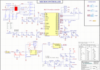
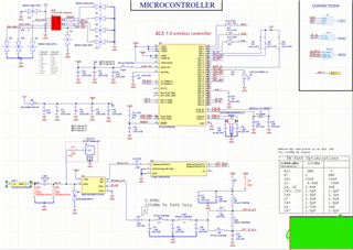
I am working with a new application and I am using the CC2652P1FRGZR considering the 20dbm PA. So, I have a couple of questions for that:
- Does the antenna type selection for this PA should be a PCB antenna? I was considering a chip antenna, but it seems insufficient for that PA. The antenna that I am considering as a chip antenna is the 2450AT45A0100001E. If that is not a good option, I am considering this PCB antenna https://www.ti.com/tool/LP-CC2651P3, but it would be nice to have a smaller one because the application would be for a wearable. Do you have any other recommendations?
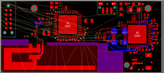
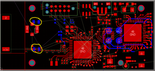
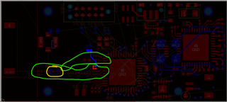
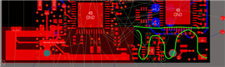
- If I use the PCB antenna, would be needed to have all of this area clean? (Green)
-
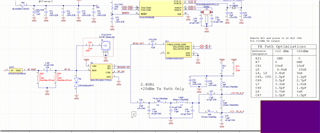
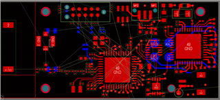
- Can you please help me review my schematic as well?
Thanks!!
Francisco