CC2538: SPI communication

Part Number: CC2538

Tool/software:

Hi team,

My customer would like to ask about the SPI.

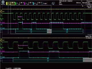
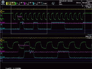
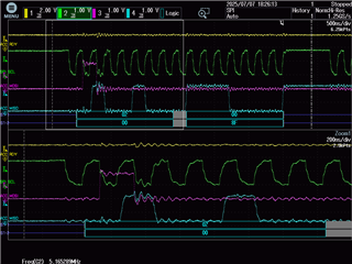
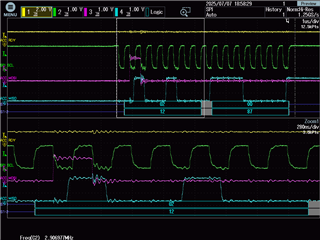
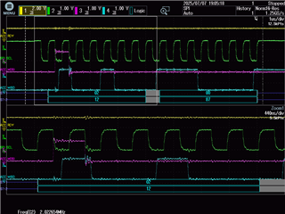
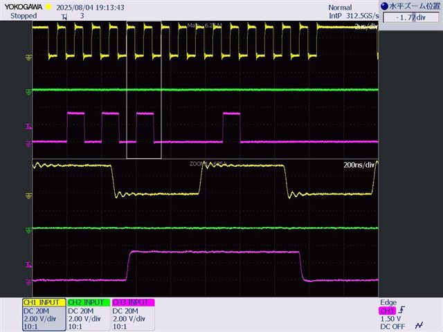
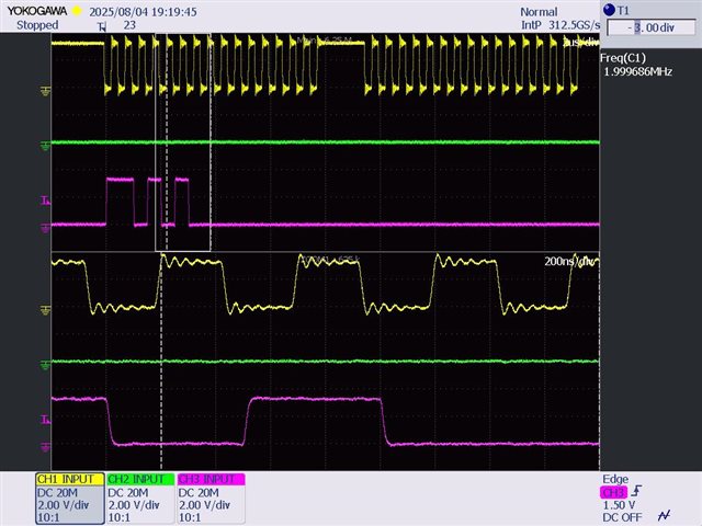
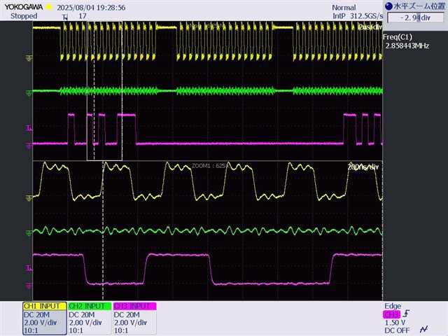
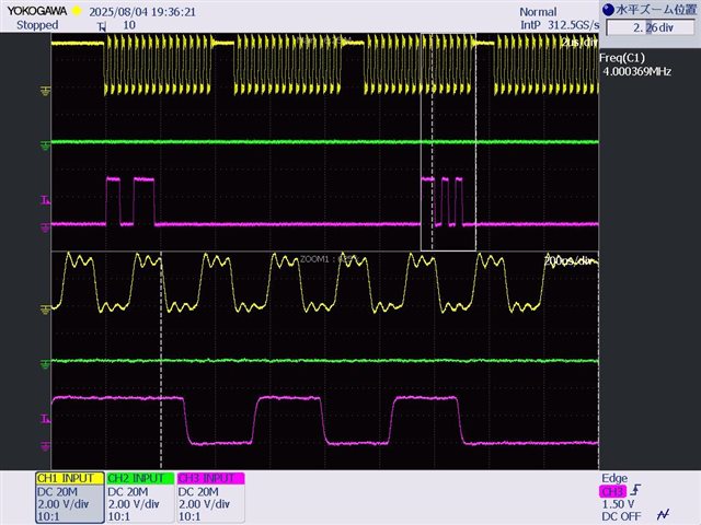
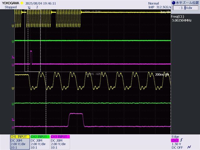
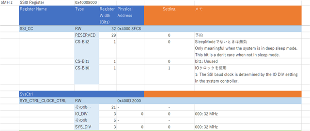
The cc2538 is used as a slave for SPI communication, but there is a problem when communicating at 5MHz.

The attached User’s Guide does not seem to describe the setup/hold time for SPI communication (19.4.4.2+).

On the other hand, there is a description of MicroWire (Figure 19-12.), is it the same as here?

It would be appreciated it if you could send us any documentation on timing characteristics such as setup/hold time of SPI communication.

CC2538swru319c.pdf

Best regards,

Kenley

  • Hi Kenley,

    I understand the CC2538 User's Guide states that the system clock or the PIOSC must be at least six times faster than the SSIClk for slave/peripheral SSI modes, and this would be true in the case that 32 MHz divided by six is greater than 5 MHz, however it is not a clean division.  Is the customer experiencing any issues when using the SPI slave at 2 or 4 MHz?  Can they provide any oscilloscope or logic analyzer screenshots of the communication lines, and are they testing on a TI EVM or custom hardware?

    Regards,
    Ryan

  • Hi Kenley,

    1. Regarding Microwire, it is a subset of SPI where


    "...the MICROWIRE format uses a special master-slave messaging technique that operates at half-duplex. In this mode, when a frame begins an 8- bit control message is transmitted to the off-chip slave. During this transmit, no incoming data is received by the SSI. After the message is sent, the off-chip slave decodes it and, after waiting one serial clock after the last bit of the 8-bit control message is sent, responds with the requested data. The returned data can be 4 to 16 bits long, making the total frame length anywhere from 13 to 25 bits."

    2. Unfortunately, SPI timings are not included in the datasheets of older devices because these types of issues are typically resolved using a lower clock speed or slightly increasing the hold/setup time. Going forward, we are pushing to add SPI timings to the datasheet on newer devices.

    Best regards,

    Bun

  • Hi Ryan and Bun,

    Thank you for your support.

    Let me share to you the feedback from customer.

    No communication error has occurred at 4MHz. When I checked the waveforms of SCL and MISO with the oscilloscope, it seemed that they were communicating at a timing that would not be strange if a communication error occurred.

    The waveform of the communication line was collected by the oscilloscope according to the communication speed, and I will send you a screenshot.

    ・ Speeds: 1 MHz, 2 MHz, 3 MHz, 4 MHz, 5 MHz

    Master/Slave: Camera/cc2538

    Communication waveform 2ch: SCL 3ch: MOSI 4ch: MISO (setting 0x12/0x87)

    You can see that the timing is off as the communication speed increases.
    In addition, the related SSI register setting values are summarized in Excel, so please check them together.

    CC2538_SSI_RegisterSetting.xlsx

  • You can see that the timing is off as the communication speed increases.

    Are you referring to the rise/fall times as compared to the period/duty cycle?  Returning to a previous question.

    are they testing on a TI EVM or custom hardware?

    Has the hardware been submitted to SIMPLELINK-2-4GHZ-DESIGN-REVIEWS? 

    No communication error has occurred at 4MHz.

    This is adequate enough to not suspect the SSI register settings, and is a possible tradeoff if the SCLK waveform cannot be improved.

    Regards,
    Ryan

  • Hi Ryan,

    Here is the feedback from customer.

    MOSI and MISO data are read at the rising edge of SCL.
    And they are evaluating usinbg their custom hardware.

    But even if the communication speed increases, the rise/fall timing of the data does not deviate with respect to the rising edge of SCL, and there seems to be sufficient setup/hold time.
    On the other hand, as the communication speed of MISO increases, the rise/fall timing of the data seems to be delayed in relation to the rise of SCL, and the normal value is not read at the rise timing of SCL.
    Especially for the 4MHz and 5MHz waveforms, the rise and fall timing of the MISO is completely off by half a period, so unintended values should be read.

    Best regards,

    Kenley

  • MOSI and MISO data are read at the rising edge of SCL.

    With the SCLK high during inactivity this is configured as SPO = 1 (SCLK inactive high) and SPH = 1 (data captured on trailing edge)

    Especially for the 4MHz and 5MHz waveforms, the rise and fall timing of the MISO is completely off by half a period, so unintended values should be read.

    The oscilloscope shows that the devices are operating at 1.8 V, and 2 V is the minimum operating voltage of the CC2538.  Most of the specs in the Datasheet and TRM assume an operating voltage of 3 V, so operating at or under the minimum operating voltage will require tradeoffs.  TI sells level shifters and boost converters for the customer's next hardware design.

    Regards,
    Ryan

  • Hi Ryan

    Thank you for your feedback.

    Sorry for the lacking information

    The waveform of the oscilloscope customer sent the other day was taken from the camera side of the 1.8V drive, not the waveform of the cc2538 side of the 3.3V drive.

    The 3.3V<-> 1.8V level shifter uses:

    ・ SCK, MOSI: SN74AUP1T08DCK

    MISO: SN74AUP2G08YZP (using 2ch)

    Best regards,

    Kenley

  • Thanks for the explanation Kenley, now it makes more sense that the CC2538 device is capable of performing under these conditions.  The existing level shifters had not been considered before.  Are there any oscilloscope screenshots on the CC2538 side for comparison of the rise/fall times?

    Regards,
    Ryan

  • Hi Ryan,

    Customer has shared the oscilloscop screenshots on the CC2538 side.

    1 channel (yellow) is CLK and 3 channel (pink) is MISO (CC2538 output signal).

    Since the line is drawn from the housing, there is a ringing of CLK in particular, but from a timing point of view, I think it is not much different from the waveform sent before.

    What do you think ?

    Best regards,

    Kenley

  • I think at 5 MHz the CC2538 does not appear to be appropriately changing the MISO line in time relative to the CLK speed.  I don't believe there are any changes from the SPI registers which would affect this.  I don't have the hardware or time with which to recreate this observation.  4 MHz may have to suffice.

    Regards,
    Ryan

  • Hi Ryan,

    Thank you for your support.

    So what do you recommend for customer to troubleshoot this issue ? 

    Best regards,

    Kenley

  • The excel sheet shows that the SSI_CC register is using SYS DIV for deep sleep (bit 0) and IO DIV for PIOSC (bit 2).  Have the customer confirm that the SYS_CTRL_CLOCK_CTRL register has IO_DIV and SYS_DIV bits set to 0x0 for a 32 MHz clock.  This is also going to require the OSC bit to select the 32-MHz crystal oscillator (value zero).  If not clear before, the 32 MHz crystal oscillator sourcing the SYS and IO clocks will be a requirement to achieve the highest SPI baud rates.

    Regards,
    Ryan

  • Hi Ryan,

    Let me clarify. I do not really get what you meant.

    Could you please elaborate ?

    Customer's settings for SSI_CC register is using SYS DIV for deep sleep (bit 0) and IO DIV for PIOSC (bit 2) as following.

    And for SYS_CTRL_CLOCK_CTRL register , it is 0 for both IO_DIV and SYS_DIV.

    In this case, what do you mean by the OSC bit is required to select the 32-Mhz crystal oscillator and If not clear before, the 32 MHz crystal oscillator sourcing the SYS and IO clocks will be a requirement to achieve the highest SPI baud rates.?

    Best regards,

    Kenley

  • the CC2538 User's Guide states that the system clock or the PIOSC must be at least six times faster than the SSIClk for slave/peripheral SSI modes, and this would be true in the case that 32 MHz divided by six is greater than 5 MHz, however it is not a clean division.

    "The PIOSC is used as the source for the SSIClk when the CS field in the SSI Clock Configuration (SSI_CC) register is configured to 0x1. For master mode, the system clock or the PIOSC must be at least two times faster than the SSIClk. For slave mode, the system clock or the PIOSC must be at least six times faster than the SSIClk."

    It is important to confirm that the SYS/IO clocks, whichever is supplying PIOSC, is not being divided from the original 32 MHz as this is crucial for SPI timing purposes as mentioned in the TRM (as the default value is listed as 0x1).  I apologize as I hadn't realized that those values were already provided at the bottom of the Excel spreadsheet.  I assume OSC is zero as well?  It should be confirmed that 32 MHz is sourcing the SPI, otherwise I don't have additional ideas to share.

    Regards,
    Ryan

  • Hi Ryan,

    The OSC of the SYS_CTRL_clock_CTRL register is set to “0” immediately after startup. So, is there an understanding that the SPI source clock is 32 MHz?

    In addition, because it is in slave mode, 32 MHz / 5 MHz = 6.4 times, which is more than 6 times.

    Best regards,

    Kenley

  • I suppose as a test you could change to SPI master mode and send out a byte, and if the SPI clock aligns with your CPSDVSR and SCR settings then you know that your clock source is as expected.

    Is the device in any low-power modes before receiving the SPI bytes, and if so does behavior improve if the device is kept in active mode?

    Regards,
    Ryan

  • Hi Ryan,


    Thank you for your support.

    Customer requested that could you please describe the specific register name and setting value for the items to be checked?

    For example, "Change to SPI master mode (set register on **** to 0x**)" etc.

    This is because customer wants to eliminate mistakes on register settings and procedures to save resources.

    And for the following question, it stays in active mode since it was powered on.

    Is the device in any low-power modes before receiving the SPI bytes, and if so does behavior improve if the device is kept in active mode?

    Best regards,

    Kenley

  • This would involve clearing bit 2 (MS) of the SSI_CR1 register.  You would then need to have the SPI start a transaction to monitor the CLK line, which can be accomplished through referencing a code example.

    Regards,
    Ryan

  • Hi Ryan,

    CC2538 SPI communicates with the main (camera).

    It is going to take time to replace the master/slave on the camera side.

    Customer would like to confirm whether anything else they can check/try out other than this master/slave swap?

    Maybe using EVM available ?

    Thank you in advance,

    Kenley

  • Just to be clear, I only most recently asked for the CC2538 to send a byte under the master configuration as a test to verify the maximum clock settings.  It was not a suggestion to permanently change the CC2538 into the master device in this environment.  You could try to use TI EVMs to verify whether communicating at a higher SPI clock frequency with this setup is possible.

    Regards,
    Ryan